Solid-state image sensor and method for fabricating the same

a solid-state image sensor and image sensor technology, applied in the field of solid-state image sensors, can solve problems such as operation defects, and achieve the effects of improving intra-plane uniformity, less fabrication fluctuations, and the same saturated charge amoun

Active Publication Date: 2006-10-10
FUJITSU SEMICON LTD
View PDF4 Cites 22 Cited by
  • Summary
  • Abstract
  • Description
  • Claims
  • Application Information

AI Technical Summary

Benefits of technology

[0012]An object of the present invention is to provide a structure of the solid-state image sensor comprising a color pixel array unit formed in the usual well and a black pixel array unit formed in an inner well of the double well, which ensures the compatibility with the fabrication process of the peripheral circuit transistors while realizing high sensitivity of the pixels, and a method for fabricating the solid-state image sensor having such the structure.
[0015]According to the present invention, in the solid-state image sensor, the pixel array unit is formed in a usual well, and the black pixel array is formed in an inner well of a double well, a buried impurity diffused region is provided between the photodiode of the black pixel and the outer well of the double well, whereby the photodiode and the outer well of the double well can be isolated from each other without failure. The buried impurity diffused region is not formed below the photodiode of the color pixel, whereby the depletion layer of the photodiode of the color pixel can extend deep in the substrate, and accordingly, the isolation between the photodiode and the outer well of the double well can be ensured without sacrificing the sensitivity of the photodiode of the color pixel.
[0016]In the color pixel, the peripheral end of the buried diffused layer of the photodiode and the peripheral end of the buried impurity diffused region with the color pixel formed in are sufficiently spaced from each other, whereby the depletion layer of the photodiode can extend sufficiently deep into the substrate. This increases the sensitivity of the photodiode.
[0018]The buried impurity diffused region to be formed in the pixel array unit is formed by ion implantation in a random direction, whereby the depth-wise distribution of the impurity has improved intra-plane uniformity, and the pixels can few fabrication fluctuations. The buried impurity diffused region in the peripheral circuit unit is formed by ion implantation in the direction normal to the substrate, whereby fluctuations of the device characteristics due to offsets of ion implanted parts and variations of the implanted depth near the photoresist end can be prevented.
[0019]A heavily doped region is formed on the bottom of the buried diffused layer of the photodiode of the black pixel, or the concentration of the buried impurity diffused region formed below the photodiode of the black pixel is made lower than a concentration in the rest region, whereby the potential of the photodiode of the black pixel can be made deep. This permits the potential depth of the photodiode of the black pixel to be approximate to the potential depth of the photodiode of the color pixel, and substantially the same saturated charge amount as that of the color pixel can be realized.
[0020]An impurity diffused region extended from the surface down to the vicinity of the bottom of the device isolation film is provided in the region between the read transistor formed region and the region between the photodiode and the device isolation film, whereby the ability of the isolation between the photodiode and the device isolation film can be further increased.

Problems solved by technology

The buried n-well and the buried n-type layer of the photodiodes are accordingly insufficiently electrically isolated, with a worst result that both may be electrically connected, causing operational defects.

Method used


Image

  • Solid-state image sensor and method for fabricating the same
  • Solid-state image sensor and method for fabricating the same
  • Solid-state image sensor and method for fabricating the same

Examples


first embodiment

[0039][A First Embodiment]

[0040]The solid-state image sensor and the method for fabricating the same according to a first embodiment of the present invention will be explained with reference to FIGS. 1 to 20.

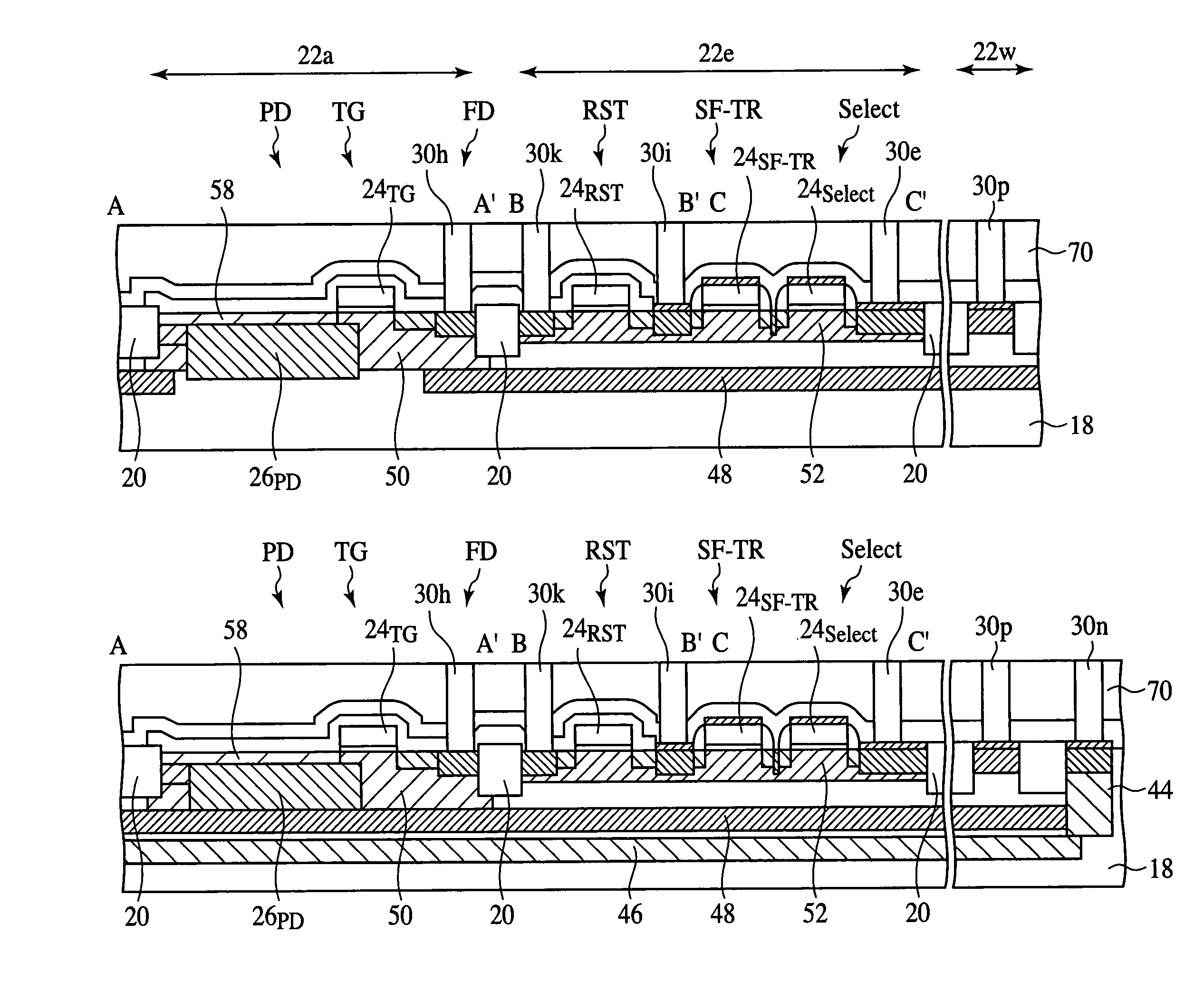
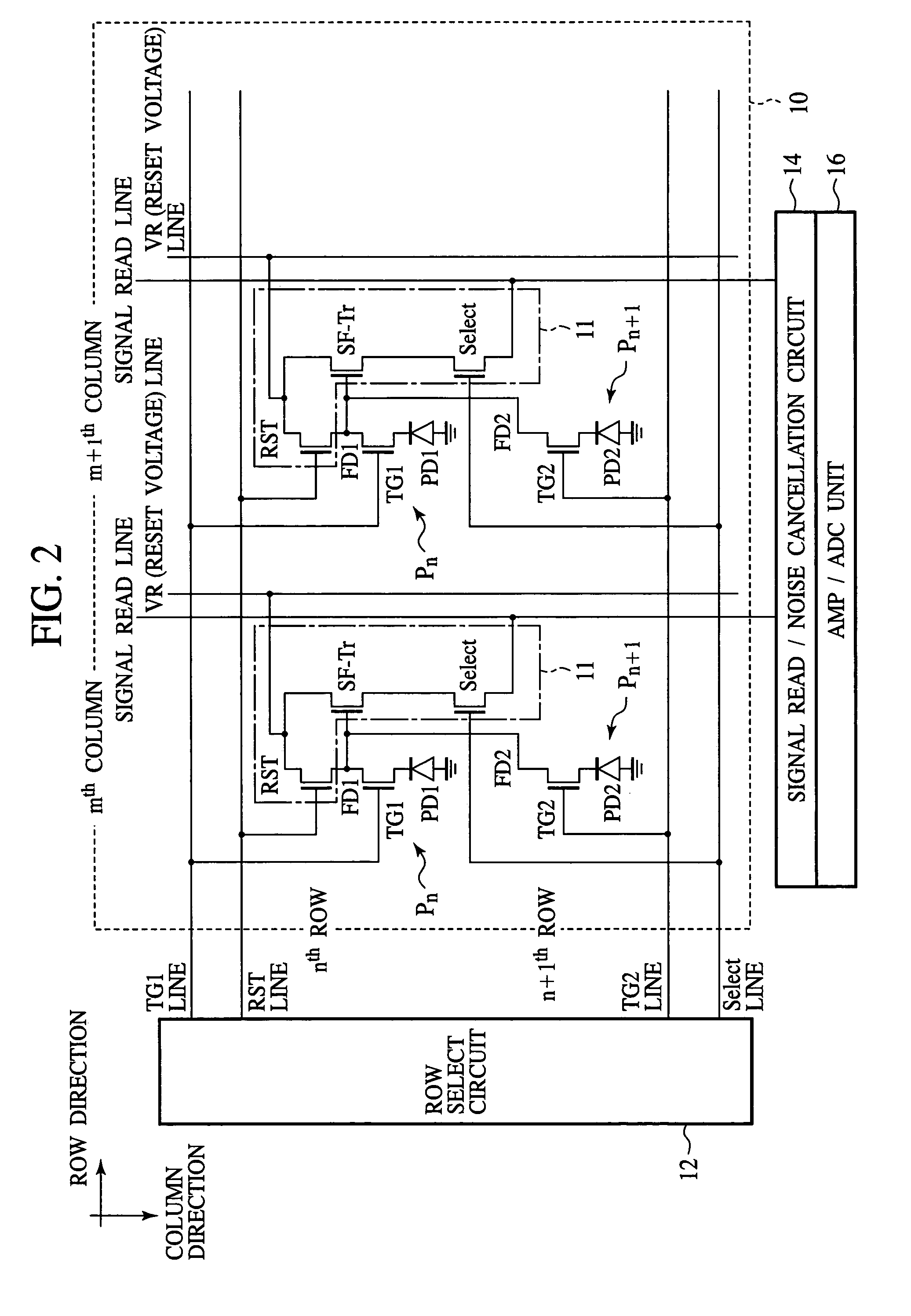
[0041]FIG. 1 is a plan view of a chip image of the solid-state image sensor according to the present embodiment. FIG. 2 is a circuit diagram of the pixel array unit of the solid-state image sensor according to the present embodiment. FIGS. 3–6 are plan views of the solid-state image sensor according to the present embodiment, which show the structure thereof. FIGS. 7A–7B are diagrammatic sectional views of the solid-state image sensor according to the present embodiment, which show the structure thereof. FIG. 8 is a graph of depth-wise changes of the potential of the region for a photodiode formed in of the solid-state image sensor according to the present embodiment. FIGS. 9A and 9B are views of the extension of the depletion layer of the photodiode. FIGS. 10A–17D are sectional...

second embodiment

[0104]In the color pixel array unit 10a, the buried p-type layer 48 is not formed either in the region for the transfer transistor TG formed in, because the end of the photoresist film used in forming the buried p-type layer 48 located near the transfer transistor TG may affect the impurity profile of the channel portion of the transfer transistor TG (see second embodiment).

[0105]FIG. 8 is a graph of depth-wise changes of the potential in the region for the photodiode PD formed in. In FIG. 8, the solid line indicates those of the color pixel, and the dotted line indicates those of the black pixel.

[0106]As shown, in the black pixel, because of the buried p-type layer 48 buried below the buried n-type layer 26PD, the potential depth is smaller by about 0.3–0.4 V in comparison with that of the color pixel. Accordingly, the charge amount (saturated charge amount) stored in the photodiode PD corresponds to ˜9000 in color pixels and ˜5000 in black pixels under the well conditions of the p...

third embodiment

[0179][A Third Embodiment]

[0180]The solid-state image sensor and the method for fabricating the same according to a third embodiment of the present invention will be explained with reference to FIGS. 24A to 25. The same members of the present embodiment as those of the solid-state image sensor and the method for fabricating the same according to the first and the second embodiments shown in FIGS. 1 to 23B are represented by the same reference numbers not to repeat or to simplify their explanation.

[0181]FIGS. 24A and 24B are diagrammatic sectional views of the solid-state image sensor according to the present embodiment, which show a structure thereof. FIG. 25 is a graph of depth-wise changes of the potential in the region for a photodiode to be formed in of the solid-state image sensor according to the present embodiment.

[0182]In the solid-state image sensor according to the first and the second embodiments, the buried n-type layer 26PD is formed under the same conditions for the ph...


PUM


Abstract

A solid-state image sensor comprises a semiconductor substrate of a first conductivity type having a color pixel region and a black pixel region; a first well of the first conductivity type formed in the color pixel region; a second well of the first conductivity type formed in the black pixel region; a third well of a second conductivity type formed, surrounding the second well and isolating the second well from the rest region of the semiconductor substrate; a color pixel formed in the first well in the color pixel region and including a first photodiode and a first read transistor for reading a signal generated by the first photodiode; and a black pixel formed in the second well in the black pixel region and including a second photodiode and a second read transistor for reading a signal generated by the second photodiode. The first well includes a first buried impurity doped layer of the first conductivity type formed in a bottom thereof in a region where the first read transistor is formed. The second well includes a second buried impurity doped layer of the first conductivity type formed in a bottom thereof in a region where the second photodiode is formed and a region where the second read transistor is formed.

Description

CROSS-REFERENCE TO RELATED APPLICATIONS[0001]This application is based upon and claims the benefit of priority from the prior Japanese Patent Application No. 2004-209681, filed on Jul. 16, 2004, the entire contents of which are incorporated herein by reference.BACKGROUND OF THE INVENTION[0002]The present invention relates to a solid-state image sensor formed of CMOS and a method for fabricating the same.[0003]As a solid-state image sensor using semiconductor materials, an image sensor formed of CMOS (CMOS image sensor) is known.[0004]The CMOS image sensor includes a pixel unit shielded from light, which are called a black pixel unit (also optical black unit) in addition to a light receiving unit of color pixel unit. The black pixel unit is for generating a reference value of a pixel signal in a dark state for the prevention of changes of a signal level due to temperature changes, etc. Accordingly, it is preferable that the black pixel unit is formed isolatable from noises of the sur...

Claims


Application Information

Patent Timeline
Patent Type & Authority Patents(United States)
IPC IPC(8): H01L31/09H01L27/146H04N5/335H04N5/361H04N5/369H04N5/374
CPCH01L27/14609H01L27/14641H01L27/14689H01L27/1463H01L27/14603H01L27/14623H01L27/14645H01L27/14H01L27/146H01L31/10
Inventor OHKAWA, NARUMI
Owner FUJITSU SEMICON LTD
Why Eureka
Try Eureka