Flash memory cell and methods for programming and erasing

US7120063B1Active Publication Date: 2006-10-10MONTEREY RES LLC

Image

  • Flash memory cell and methods for programming and erasing
  • Flash memory cell and methods for programming and erasing
  • Flash memory cell and methods for programming and erasing

Examples


Embodiment Construction

[0025]One or more implementations of the present invention will now be described with reference to the drawings, wherein like reference numerals are used to refer to like elements throughout.

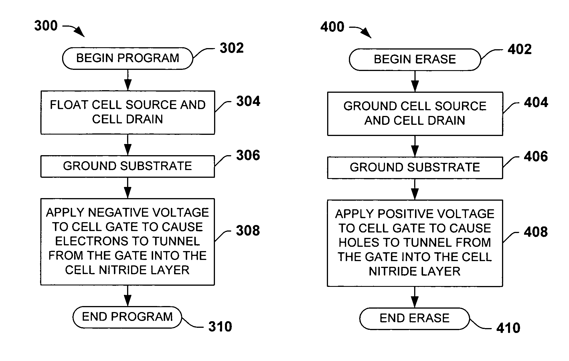
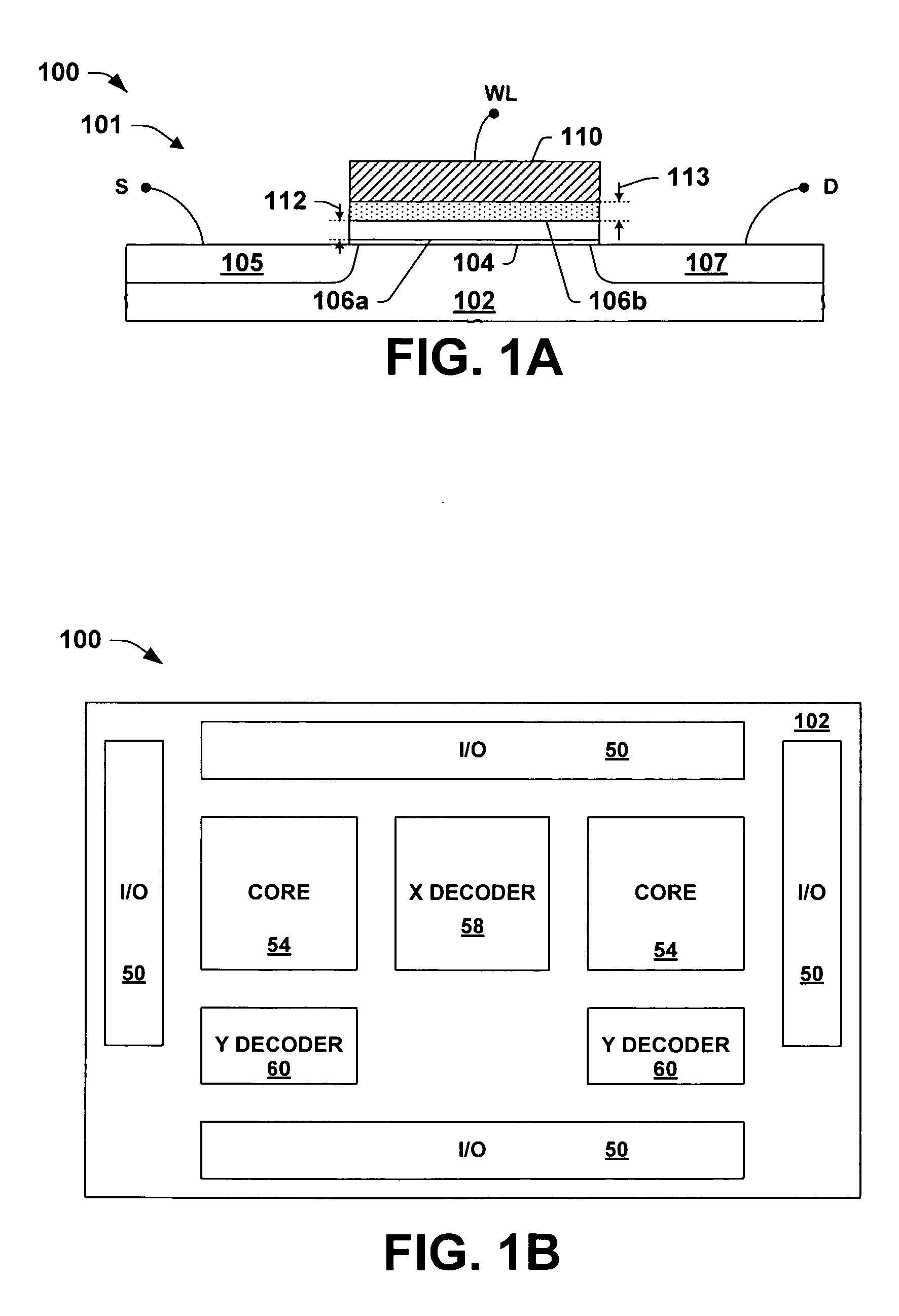
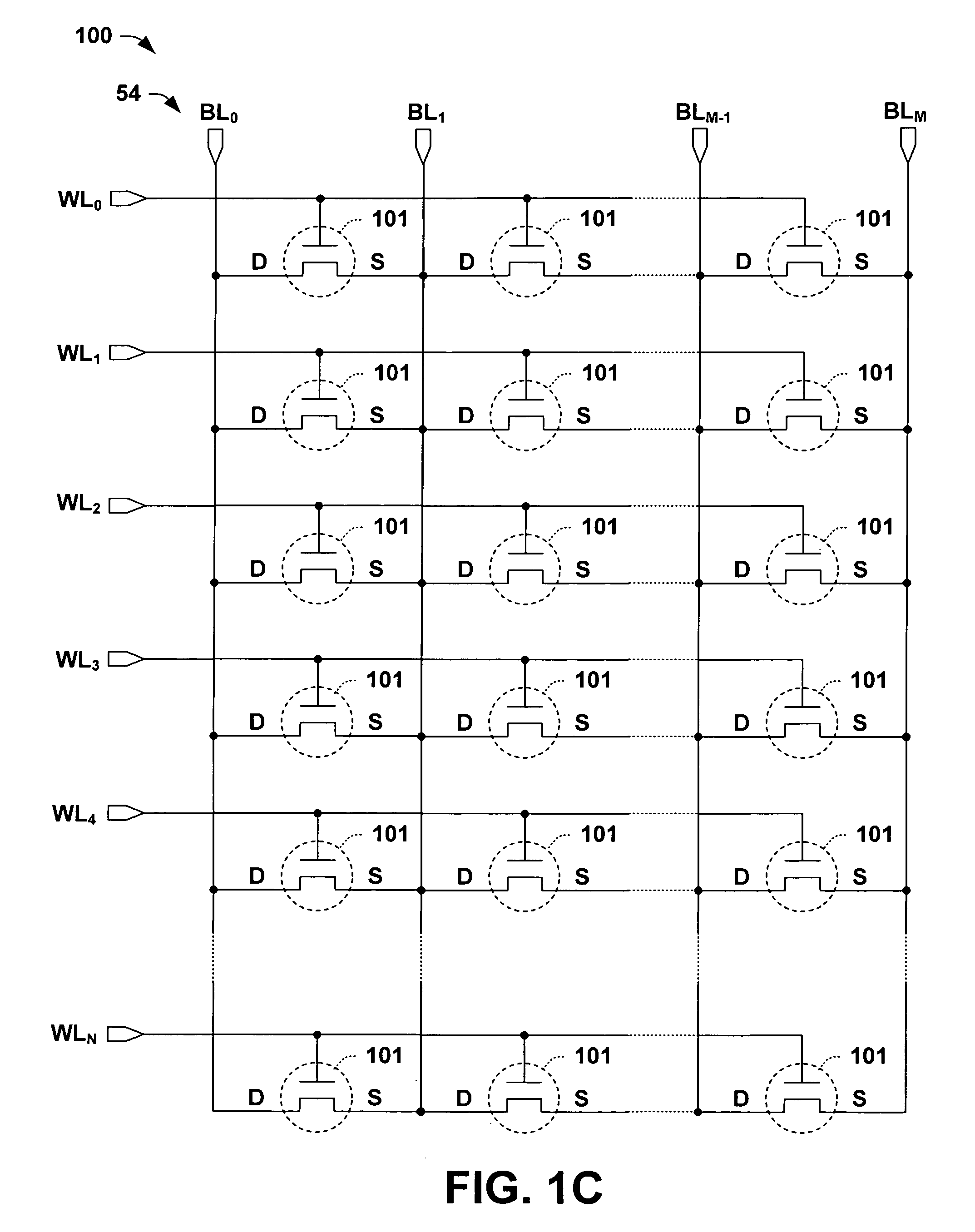
[0026]The invention provides flash memory cells comprising a dielectric material formed above a substrate channel region, a charge trapping material formed over the dielectric material, and a control gate formed over the charge trapping material. As used herein, a structure that is formed over another structure is in contact therewith, whereas a structure formed above another structure may, but need not, be in contact therewith. The cells may be programmed by directing electrons from the control gate into the charge trapping material to raise the cell threshold voltage and may be erased by directing electrons from the charge trapping material into the control gate to lower the threshold voltage. The invention may be employed to facilitate scaling efforts, as well as to enhance device endurance a...


PUM


Abstract

Flash memory cells are presented which comprise a dielectric material formed above a substrate channel region, a charge trapping material formed over the dielectric material, and a control gate formed over the charge trapping material. The cell may be programmed by directing electrons from the control gate into the charge trapping material to raise the cell threshold voltage. The electrons may be directed from the control gate to the charge trapping material by coupling a substrate to a substrate voltage potential, and coupling the control gate to a gate voltage potential, where the gate voltage potential is lower than the substrate voltage potential. The cell may be erased by directing electrons from the charge trapping material into the control gate to lower a threshold voltage of the flash memory cell, such as by coupling the substrate to a substrate voltage potential, and coupling the control gate to a gate voltage potential, where the gate voltage potential is higher than the substrate voltage potential.

Description

RELATED APPLICATIONS[0001]This application is related to U.S. patent application Ser. No. 10 / 841,788, filed on May 7, 2004, entitled FLASH MEMORY CELL WITH THIN UPPER DIELECTRIC, the entirety of which is hereby incorporated by reference as if fully set forth herein.FIELD OF INVENTION[0002]The invention is generally related to the field of memory devices and more particularly to flash memory cells and methods for programming and erasing the same.BACKGROUND OF THE INVENTION[0003]Flash memory is a non-volatile type of memory which can be rewritten and retain its data content without power. Flash and other types of electronic memory devices are constructed of memory cells that individually store and provide access to data. A typical memory cell stores a single binary piece of information referred to as a bit, which has one of two possible states. The cells are commonly organized into multiple cell units such as bytes having eight cells and words having sixteen or more such cells, usuall...

Claims


Application Information

Patent Timeline
10 Oct 2006
Publication
US7120063B1
IPC
G11C11/34; G11C16/04
CPC
G11C16/0466; G11C16/0491; H01L21/28282; H01L29/66833; H01L29/40117
Inventors
LIU, ZHIZHENG; LIU, ZENGTAO