Wiring board and circuit module

a circuit module and wiring board technology, applied in the field of wiring boards, can solve the problems of difficult miniaturization, considerable problem, and known technology difficulty in meeting the demand for cost reduction

Inactive Publication Date: 2006-10-17
SONY CORP
View PDF3 Cites 6 Cited by
  • Summary
  • Abstract
  • Description
  • Claims
  • Application Information

AI Technical Summary

Benefits of technology

[0035]Since an IC and a passive component are provided in addition to the bare IC described above, the circuit module can provide the same advantages as those of the wiring board of the present invention.

Problems solved by technology

Wireless communication ICs (semiconductor integrated circuit devices) for transmitting / receiving high-frequency signals and ICs for processing high-speed digital signals are susceptible to noise radiated from the surroundings, and the ICs also can be radiation-noise generating sources relative to other devices.
The known technology shown in FIG. 1, however, requires the attachment of the shield cap 108 for covering the IC (e.g., an RF-IC) 107 to provide electrostatic shielding, thus posing a problem in that it is difficult to achieve miniaturization.
Thus, since the known technology shown in FIG. 1, which requires the attachment of the shield cap 108, has difficulty in fulfilling the demand for miniaturization, it has a considerable problem.
Further, since the attachment of the shield cap 108 requires time and cost, the known technology has difficulty in meeting a demand for cost reduction.
The shield cap 108 also has a disadvantage in that it cannot electrostatically shield the bottom-side of the IC 107.
Japanese Unexamined Patent Application Publication No. 2001-77537, however, does not provide electrostatic shielding against noise penetrating the RF-IC 107 from its side surfaces, which therefore does not provide a sufficient electrostatic shielding effect.

Method used


Image

  • Wiring board and circuit module
  • Wiring board and circuit module
  • Wiring board and circuit module

Examples


first embodiment

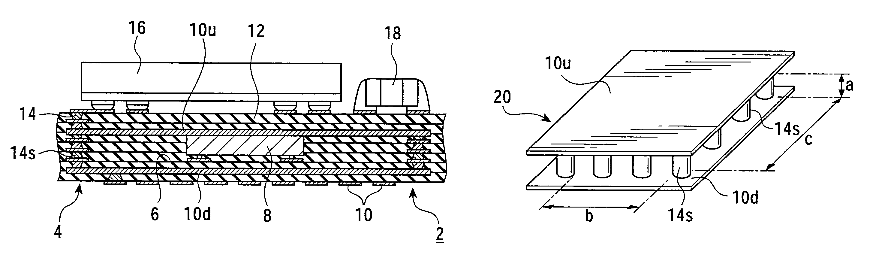
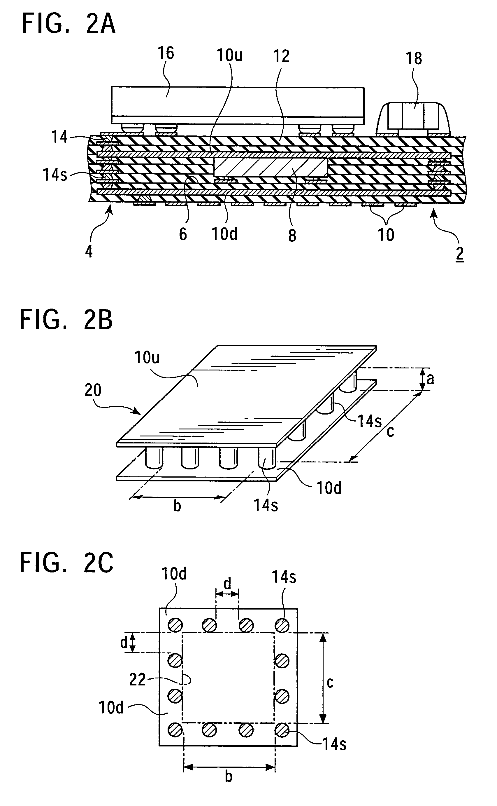
[0043]FIGS. 2A to 2C illustrate a circuit module according to the present invention. Specifically, FIG. 2A is a cross-sectional view of the circuit module, FIG. 2B is a perspective view showing a shield cage in a wiring board included in the circuit module, and FIG. 2C is a plan sectional view of the shield cage.

[0044]In FIG. 2A, reference numeral 2 indicates a circuit module, for example, a small-power wireless communication module employing the Bluetooth ISM (Industrial, Scientific and Medical) band (2.4 GHz band), and reference numeral 4 indicates a wiring board. The wiring board 4 has an IC housing space 6, in which an RF-IC 8, such as an IC for a transceiver Modem, is housed.

[0045]Reference numeral 10 indicates wiring films for the wiring board 4. The wiring films 10 are made of metal, such as copper. Reference numeral 12 indicates an insulating layer, which is made of a resin. Reference numeral 14 indicates via-holes, which extend through interlayer insulating films and which ...

second embodiment

[0058]FIGS. 3A and 3B illustrate a circuit module according to the present invention. Specifically, FIG. 3A is a cross sectional view of the circuit module, and FIG. 3B is a perspective view of a shield cage in a wiring board included in the circuit module, the shield cage being shown upside down. Reference numeral 2a indicates a circuit module according to the present embodiment. The circuit module 2a is analogous to the circuit module 2 shown in FIG. 2, except that a hole 24 is provided in a lower shield wiring film 10d.

[0059]When a ground line is provided in the vicinity of an active surface of an IC and the potential thereof affects the characteristics of the IC, the hole 24 serves to prevent the potential from affecting the IC. When the longitudinal side of the hole 24 has a length of λg / 2 or more, the hole 24 acts as a slit antenna to cause reflection. Thus, it is preferable that the longitudinal side be set to less than λg / 2.

[0060]Reference numeral 26 indicates a printed wir...


PUM


Abstract

A wiring board houses a bare radio-frequency IC. Shield wiring films are provided above and below the IC. A plurality of shield interlayer-connection conductor films, i.e., shield via-holes, is provided so as to surround the IC. The shield wiring films and the shield interlayer-connection conductor films define a shield cage, which can electrostatically shield the IC. Thus, there is no need to attach a shield cap.

Description

BACKGROUND OF THE INVENTION[0001]1. Field of the Invention[0002]The present invention relates to a wiring board that has a plurality of wiring films, which are provided between interlayer insulating films, and interlayer-connection conductor films, which extend through the interlayer insulating films and provide electrical connections between the wiring films at different layers, and that houses at least one bare semiconductor integrated circuit device. The present invention also relates to a circuit module having another semiconductor integrated circuit device and a passive component that are mounted on the wiring board.[0003]2. Description of the Related Art[0004]Wireless communication ICs (semiconductor integrated circuit devices) for transmitting / receiving high-frequency signals and ICs for processing high-speed digital signals are susceptible to noise radiated from the surroundings, and the ICs also can be radiation-noise generating sources relative to other devices.[0005]Accor...

Claims


Application Information

Patent Timeline
Patent Type & Authority Patents(United States)
IPC IPC(8): H01L23/552H01L29/00H01L39/00H01L23/00H01L23/498H05K1/02H05K1/18
CPCH01L23/552H05K1/0218H01L23/49805H01L2224/16H01L2924/16152H05K2201/09609H01L2924/3025H05K1/185H01L2924/19105H01L2224/05573H01L2224/05568H01L2924/00014H01L2224/05599E04G25/061
Inventor TSUKAMOTO, SOTAROKUROMIYA, SATORUHANAI, NOBUHIROHAYASHIDA, MASATO
Owner SONY CORP
Why Eureka
Try Eureka