Etching methods and apparatus and substrate assemblies produced therewith

a technology of substrate assembly and etching method, which is applied in the direction of transportation and packaging, electric discharge tubes, other domestic articles, etc., can solve the problems of difficult to etch deep har features into the substrate assembly, limited etching performance of dry etching with plasma, and insufficient wet etching production, etc., to achieve the effect of increasing the thickness of the resist layer

Inactive Publication Date: 2006-10-24
MICRON TECH INC
View PDF18 Cites 2 Cited by
  • Summary
  • Abstract
  • Description
  • Claims
  • Application Information

AI Technical Summary

Benefits of technology

[0017]In another method, a feature is etched into a substrate assembly by forming a resist layer on a surface of the substrate assembly and defining a feature on the surface by patterning the resist layer by removing the resist layer from at least a portion of the substrate assembly. The portion of the substrate assembly that is not covered by the resist layer is etched with a plasma generated in a flow of a first halogenated hydrocarbon-containing gas or gas mixture. Simultaneously with the etching of the substrate assembly, the plasma increases the thickness of the resist layer, and the feature is etched to have an aspect ratio of at least 10:1. In a further embodiment, one or more subsequent or prior etches, including a resist-consuming etch, may be performed to etch the portion of the substrate assembly that is not covered by the resist.

Problems solved by technology

A particular problem is the etching of a silicon wafer or other substrate assembly to produce damascene layers, self-aligned contacts (SACs), or trench isolation.
While wet etching is simple and inexpensive, wet etching is generally inadequate to produce HAR features because wet etches tend to etch isotropically.
In addition, it is difficult to etch deep HAR features into a substrate assembly because the etchant does not flow freely into and out of the feature.
Unfortunately, dry etching with a plasma has significant limitations.
As a result, the total etching time is limited by the time required for the plasma etch to penetrate the photoresist.
Etching deep HAR features requires thick layers of photoresist to permit long etch times, and such thick layers complicate the photolithographic patterning process.
Patterning a feature as small as about 250 nm is very difficult in such a thick layer of photoresist.
Other factors limiting plasma etching include the difficulty of providing a selected distribution of ions (charged particles) and neutral particles at the substrate surface and at the bottom of a feature being etched.

Method used


Image

  • Etching methods and apparatus and substrate assemblies produced therewith
  • Etching methods and apparatus and substrate assemblies produced therewith
  • Etching methods and apparatus and substrate assemblies produced therewith

Examples


Embodiment Construction

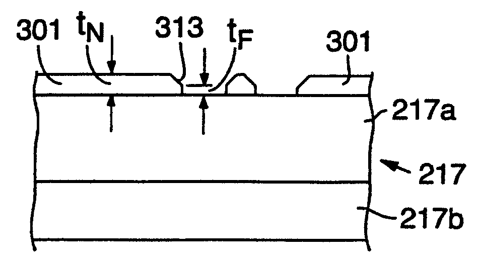
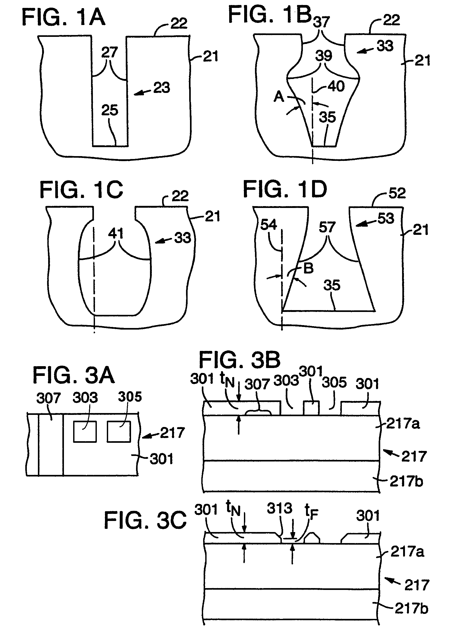
[0033]Methods, apparatus, and etched substrate assemblies are disclosed. In semiconductor manufacturing, a common starting material is a silicon wafer that is either doped or undoped. For some semiconductor devices, other wafer materials are used such as GaAs and InP. During device manufacturing, layers of various materials are applied to a surface of the wafer and circuit features are defined on the wafer. As used herein, a substrate assembly refers to a semiconductor wafer including any features or layers formed on the wafer.

[0034]The methods and apparatus disclosed are suitable for etching so-called high-aspect ratio (“HAR”) features as well as other features. As used herein, a high-aspect-ratio feature is a feature having a depth-to-width ratio of at least 5:1, wherein a depth is a dimension of a feature measured in a direction perpendicular to the etched surface of the substrate assembly, and a width is a dimension of a feature measured in a direction parallel to the etched sur...


PUM

PropertyMeasurementUnit
thicknessaaaaaaaaaa
thicknessaaaaaaaaaa
thickaaaaaaaaaa

Abstract

Methods and apparatus for etching substrates such as silicon wafers are provided. In one specific approach, a surface of the substrate assembly is covered with a resist that is patterned to define features to be etched. In this approach, the surface is then exposed to a plasma in a plasma etcher so that surface areas not covered with the resist are etched, while the thickness of the resist increases or etches at a rate that is at least ten times slower than that of the exposed areas of the surface. This etching process can be followed with a conventional plasma etch. By combining the etching that increases the resist thickness with the conventional etching of resist in which the resist thins during etching, features having high-aspect-ratios can be etched.

Description

CROSS-REFERENCE TO RELATED APPLICATIONS[0001]This application is a continuation of U.S. patent application Ser. No. 09 / 916,734, filed Jul. 26, 2001, U.S. Pat. No. 6,784,111 which is a division of U.S. patent application Ser. No. 09 / 342,677, filed Jun. 29,1999, U.S. Pat. No. 6,635,335, which are incorporated herein by reference.TECHNICAL FIELD[0002]The invention pertains to methods and apparatus for etching silicon wafers or other substrate assemblies and to substrate assemblies.BACKGROUND OF THE INVENTION[0003]The fabrication of very large-scale integrated circuits requires processes that are compatible with small feature sizes (e.g., 0.25 μm). A particular problem is the etching of a silicon wafer or other substrate assembly to produce damascene layers, self-aligned contacts (SACs), or trench isolation. These features typically require etching relatively deeply into the wafer while maintaining a small footprint on the surface of the substrate assembly, i.e., these features have a h...

Claims


Application Information

Patent Timeline
Patent Type & Authority Patents(United States)
IPC IPC(8): H01L21/311
CPCH01J37/321H01L21/3085H01L21/31116H01L21/32137H01L21/32139H01L21/76232H01L21/31144H01J2237/3345H01J2237/3347Y10T428/24479Y10S428/901Y10T428/2457
Inventor DONOHOE, KEVIN G.STOCKS, RICH
Owner MICRON TECH INC
Why Eureka
Try Eureka