Systems and methods for multi-dimensional metrology and/or inspection of a specimen

a three-dimensional metrology and specimen technology, applied in the field of three-dimensional metrology and/or specimen inspection, can solve the problems of excessive current draw through the probe card, inability to detect the presence of a specimen, etc., and achieve the effect of relaxed design tolerances and high speed scanning

Active Publication Date: 2006-10-24
KLA TENCOR TECH CORP
View PDF8 Cites 86 Cited by
  • Summary
  • Abstract
  • Description
  • Claims
  • Application Information

AI Technical Summary

Benefits of technology

[0027]In one embodiment, the method may also include scanning the specimen with full oblique illumination to form a reference image of the structure, integrating an intensity of the reference image, and reducing albedo differences between the structure and additional structures on the specimen using the reference image. In another embodiment, determining the height of the structure may include determining the height of the structure from the integrated intensities of the image and the reference image.
[0031]One advantage of the systems and methods described herein is that high speed scanning for both two-dimensional and three-dimensional data acquisition are provided. An additional advantage is that two-dimensional and three-dimensional defect detection and metrology may be performed in a single pass. A further advantage is that independent techniques and hardware systems are not required to accomplish the two-dimensional and three-dimensional data acquisitions. Furthermore, if common hardware systems are used to perform multiple tasks, then the system may include fewer components and may have more relaxed design tolerances. For example, the system may include fewer mechanical and electrical components. In addition, the systems and methods as described herein may be more sensitive, and particularly more sensitive over a relatively large field of view, than currently available systems and methods for three-dimensional data acquisition.

Problems solved by technology

Bumps that are incorrectly formed on a wafer may cause significant problems during further processing such as probing of the wafer and during use of the device.
For example, incorrectly formed bumps may damage probes on a probe card thereby causing tester downtime and incurring tester repair costs.
Incorrectly formed bumps may also bridge power and ground contacts thereby resulting in excessive current draw through a probe card.
In addition, incorrectly formed bumps may not be detected during probing and may increase the potential for failure of a packaged device.
Furthermore, probing may damage bumps especially on a wafer having a relatively high number of bumps per unit area that may require high vertical forces during testing to seat probes for proper contact.
Because currently available methods are generally not capable of simultaneous 2D and 3D data acquisition, such methods may be significantly slower than either 2D or 3D data acquisition.
In addition, 3D data acquisition may be significantly slower than 2D data acquisition thereby resulting in substantially reduced sampling for 3D in comparison to sampling for 2D.
There are several disadvantages to the moiré-type systems and methods for three-dimensional inspection of objects.
For example, these systems and methods include complex system configurations and rely on data collected from a separate reference object.
In addition, using such a sine wave pattern may yield inaccurate height measurements.
However, if the height of an object is outside of this range, the height of the object may be inaccurately reported with an error of one or more times the range of heights.
There are several additional disadvantages to currently available systems and methods for three-dimensional inspection of bumped wafers.
In addition, configurations of such systems are incompatible with rapid scanning of relatively large areas of bumped wafers.
Such disadvantages will generally lower a throughput of an inspection and metrology system.
Furthermore, such systems may be relatively complex due to the use of separate 2D and 3D data acquisition and processing systems.
This disadvantage will generally increase cost and reduce reliability of an inspection and metrology system.

Method used


Image

  • Systems and methods for multi-dimensional metrology and/or inspection of a specimen
  • Systems and methods for multi-dimensional metrology and/or inspection of a specimen
  • Systems and methods for multi-dimensional metrology and/or inspection of a specimen

Examples


Embodiment Construction

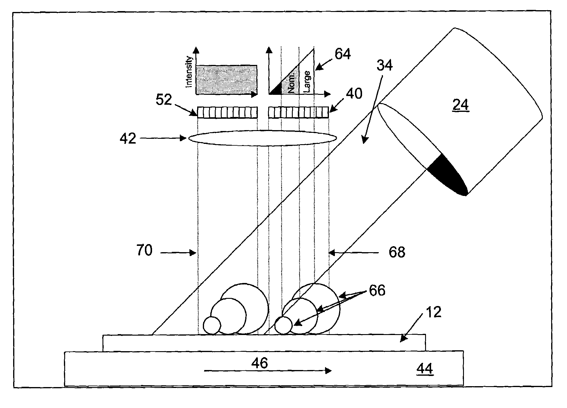
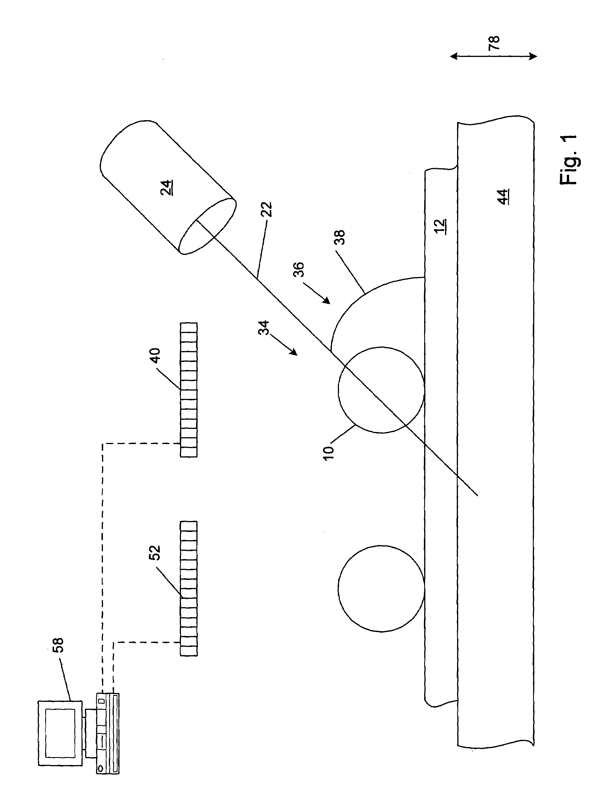
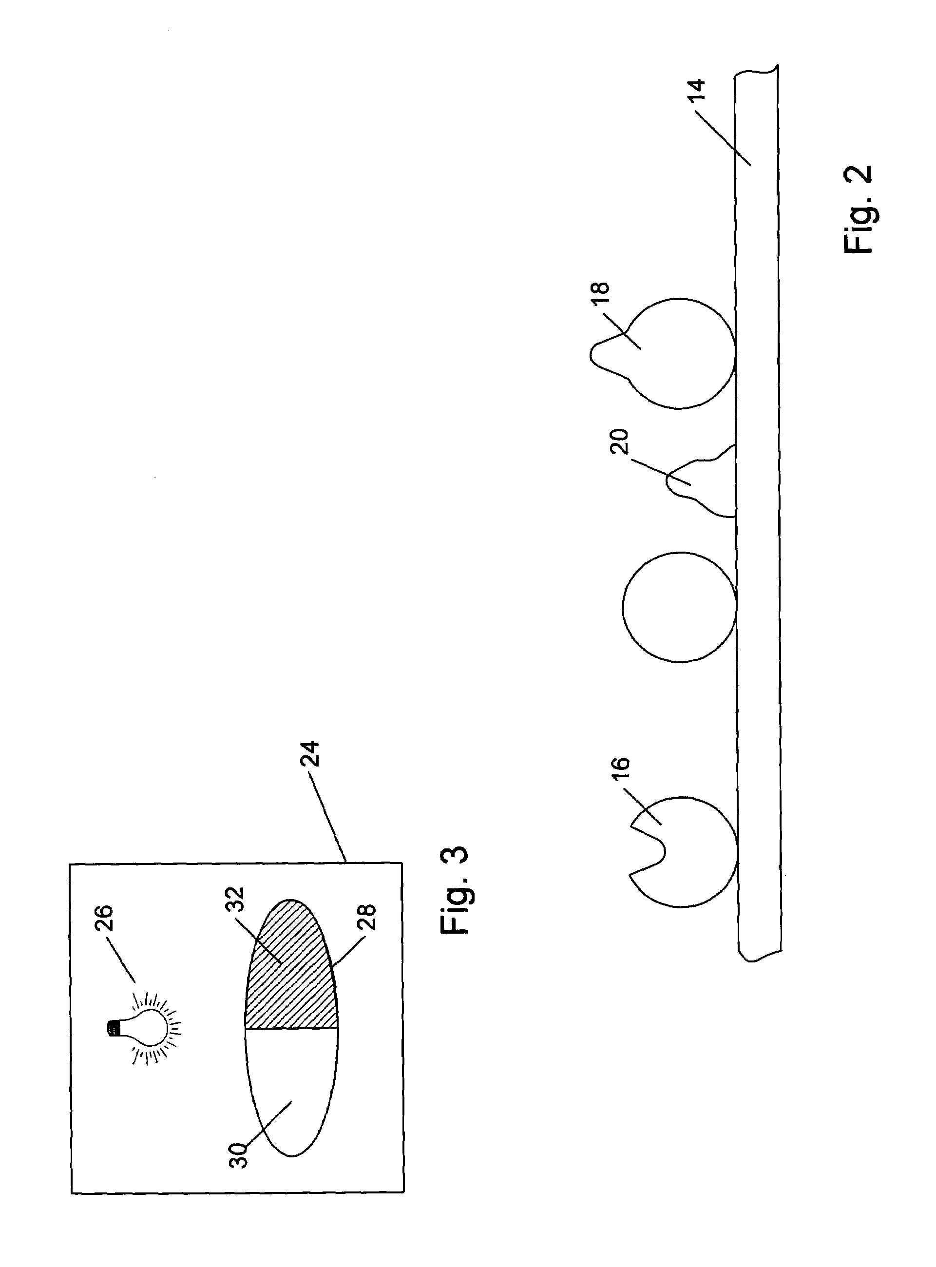
[0050]The following description generally relates to systems and methods for determining a dimension of a structure on a specimen. Various embodiments relate to a system that may include an imaging system configured to relate structure heights directly to image exposure duration, a processor configured to determine a height of a structure from exposure differences, and an imaging system coupled to a processor that provides lateral (two-dimensional) metrology and defect detection. Such a system may be configured to perform inspection and metrology in three-dimensions within the same pass.

[0051]As will be further described herein, elements that may be similarly configured in each of the embodiments illustrated in FIGS. 1–19 have been indicated by the same reference characters. It is noted that FIGS. 1–19 are not drawn to scale. In particular, the scale of some of the elements of the figures is greatly exaggerated to emphasize characteristics of the elements. It is also noted that FIGS...


PUM


Abstract

Systems and methods for multi-dimensional metrology and inspection of a specimen such as a bumped wafer are provided. One method includes scanning the specimen with partial oblique illumination to form an image of the structure, either through the normal collection angle or through an oblique collection angle. The method also includes integrating an intensity of the image and determining a height of the structure from the integrated intensity. The integrated intensity may be approximately proportional or inversely proportional to the height of the structure. In addition, the method may include scanning the specimen with bright field illumination to form a bright field image of the specimen. The method may also include determining a lateral dimension of the structure from the bright field image. Furthermore, the method may include detecting defects on the specimen from the bright field image or the obliquely-illuminated image.

Description

PRIORITY CLAIM[0001]This application claims priority to U.S. Provisional Application No. 60 / 419,793 entitled “Systems and Methods for Multi-Dimensional Metrology and / or Inspection of a Specimen,” filed Oct. 18, 2002.BACKGROUND OF THE INVENTION[0002]1. Field of the Invention[0003]The present invention generally relates to systems and methods for three-dimensional metrology and / or inspection of a specimen. Certain embodiments relate to systems and methods for metrology and inspection of a specimen such as a bumped wafer.[0004]2. Description of the Relevant Art[0005]Fabricating semiconductor devices such as logic and memory devices typically includes processing a specimen such as a wafer using a number of semiconductor fabrication processes to form various features and multiple levels of the semiconductor devices. For example, lithography is a semiconductor fabrication process that typically involves transferring a pattern to a resist arranged on a wafer. Additional examples of semicon...

Claims


Application Information

Patent Timeline
Patent Type & Authority Patents(United States)
IPC IPC(8): G01B11/02
CPCG01B11/0608G01N21/9501
Inventor WIHL, TIMHIEBERT, STEPHENKOLE, FRANKSCHMIDLEY, RICHARD
Owner KLA TENCOR TECH CORP
Why Eureka
Try Eureka