Medium pressure plasma system for removal of surface layers without substrate loss

a plasma system and medium pressure technology, applied in the field of selective removal of surface layers, can solve the problems of unwanted damage to the components of the semiconducting device or to the wafer substrate itself, the limited cooling efficiency of the apparatus effectively limited the power density of the resulting plasma, and the operation of the plasma at high energy involves very high temperatures. , the effect of high efficiency

Inactive Publication Date: 2007-10-04
UNIV HOUSTON SYST +1
View PDF8 Cites 14 Cited by
  • Summary
  • Abstract
  • Description
  • Claims
  • Application Information

AI Technical Summary

Benefits of technology

[0007] The present invention addresses the foregoing needs by providing a new approach for removing surface layers from semiconductor wafers. The present invention provides a method wherein reactant gases are activated by a medium pressure surface wave discharge. The method further involves the formation of volatile reactants in the plasma gas that can strip photoresist from the surface of a wafer. The plasma gas forms a reactive plasma jet that impinges on a substrate from which surface layers may be selectively, thus safely, etched with high efficiency. The method may be practiced in a commerically viable manner for stripping applied materials from large wafers by scanning them in front of the jet.
[0009] An embodiment of the present invention is provided as an apparatus for performing medium pressure (between about 10 Torr and about 500 Torr) plasma material removal on semiconductor wafers. The apparatus provides a system wherein reactant gases, such as O2, H2, H2O, N2, etc., may flow through a narrow discharge tube made of quartz , sapphire or other electromagnetic insensitive material, and wherein surface wave activation by an electromagnetic power source, such as a microwave or RF power source, may be applied. Additionally, a cooling system for the discharge tube using a gaseous coolant is provided, further comprising an integral cooling flange on the discharge tube, which may be attached to a cooling channel. The apparatus may further comprise a discharge nozzle from which the gas emerges from the tube and impinges on a substrate, such that resultant volatile reaction products, such as H2O, CO2, or low molecular weight hydrocarbons, may selectively strip material layers from the surface of a substrate wafer. The apparatus may further comprise a positioning system for supporting a wafer chuck, that provides wafer heating and positioning, and provides for high speed scanning of a wafer with the plasma source.
[0010] The use of surface wave discharges has the unique advantage of being able to guide the discharge from the point where excitation power is applied, to the wafer where it is used. Also, the method of providing a surface wave discharge may be practiced over a wide range of pressure without significant changes to the electromagnetic power system.
[0011] The ideal operating pressure range of the present invention is in the medium pressure regime (greater than about 10 Torr, but less than about 500 Torr). Medium pressure plasmas have the advantage that very high rates of electron-ion recombination and energetic particle thermalization may eliminate the high energy charged species present in low pressure plasmas. Eliminating these high energy species eliminates the possibility of potentially damaging substrate currents and sputter erosion. Further, plasma gas temperatures in the medium pressure regime are extremely high compared to low pressure plasmas. Higher plasma gas temperatures provide an additional source of heat in the reactive zone on the wafer, specifically there where it is most required. This focused thermal energy positively contributes to the reactive removal of organic material, wherein the reaction rate of material removal is increased, thereby increasing the speed (and so the commercial viability) of the process. In contrast, the use of low pressures (less than about 10 Torr) for this plasma jet system may not be desirable because, as pressure decreases, the geometry of the plasma jet may flare out, thereby making the “spot size” less controllable. The use of high pressures (greater than about 500 Torr) may not be advantageous because the reactive species needed for surface removal may recombine before reaching the wafer, thus reducing the effectiveness of the plasma for highly selective removal. Operation of the present invention over a wide pressure window may, however, enable atmospheric wafer exchange while the plasma source is still operating. Since ignition of the plasma normally requires low pressure (close to 1T), cycling the process pressure may be avoided if the power source can be maintained during wafer exchange at about 760 Torr (atmospheric pressure). This may avoid additionally having to vaccum pump down to low pressure for plasma ignition, and then repressurizing to medium pressure for processing each semicondutor wafer, thereby further saving valuable process time in an industrial setting.

Problems solved by technology

High energy ion bombardment may cause unwanted damage to components of the semiconducting device or to the wafer substrate itself.
However, the limited cooling efficiency of this apparatus effectively limited the power densities of the resulting plasma.
However, operating a plasma at high energy involves very high temperatures.
Once initiated, the oil-based carbon layer grows rapidly with increasing microwave exposure; eventually, catastrophic arcing takes place within the waveguide and destroys the plasma discharge tube.
Thus, oil-cooled systems are unsuitable for high energy plasma discharges.
Air-cooled high power plasma systems have been reported, but their operation was limited to atmospheric pressure, i.e. in the high pressure regime, such that the resulting plasma would not contain reactive species necessary for selective removal of organic surface layers, such as photoresist, (Y. Okamoto, High-Power Microwave-Induced Helium Plasma At Atmospheric Pressure For Determination Of Halogens In Aqueous Solution, Jap. Journ. Appl. Phys.
Once the resist layer has been subjected to ion implantation, as required for intermediate IC fabrication steps, the reaction mechanism using plasma becomes more complex.
Ion implanted resist is much more difficult to remove than unimplanted resist, since the implantation process produces a carbonized crust mixed with metal ions that exhibits extremely low intrinsic etch rates, (G K. Vinogradova et al., J. Vac. Sci. Technol.
However, these more aggressive removal methods invariably cause some degree of erosion of unprotected surfaces.
Increasingly, such losses on wafer surfaces are becoming economically unacceptable as the thickness of gate oxide and contacts continue to shrink with each new generation of ICs.

Method used


Image

  • Medium pressure plasma system for removal of surface layers without substrate loss
  • Medium pressure plasma system for removal of surface layers without substrate loss
  • Medium pressure plasma system for removal of surface layers without substrate loss

Examples


Embodiment Construction

[0021] In the following description, numerous specific details are set forth such as specific process values or parameters, etc. to provide a thorough understanding of the present invention. However, it will be obvious to those skilled in the art that the present invention may be practiced without such specific details. In other instances, well known components have been shown in block diagram form in order not to obscure the present invention in unnecessary detail. For the most part, details concerning specific semiconductor product applications and the like have been omitted inasmuch as such details are not necessary to obtain a complete understanding of the present invention and are within the skills of persons of ordinary skill in the relevant art.

[0022] Referring now to the drawings wherein depicted elements are not necessarily shown to scale and wherein like or similar elements are designated by the same reference numeral through the several views:

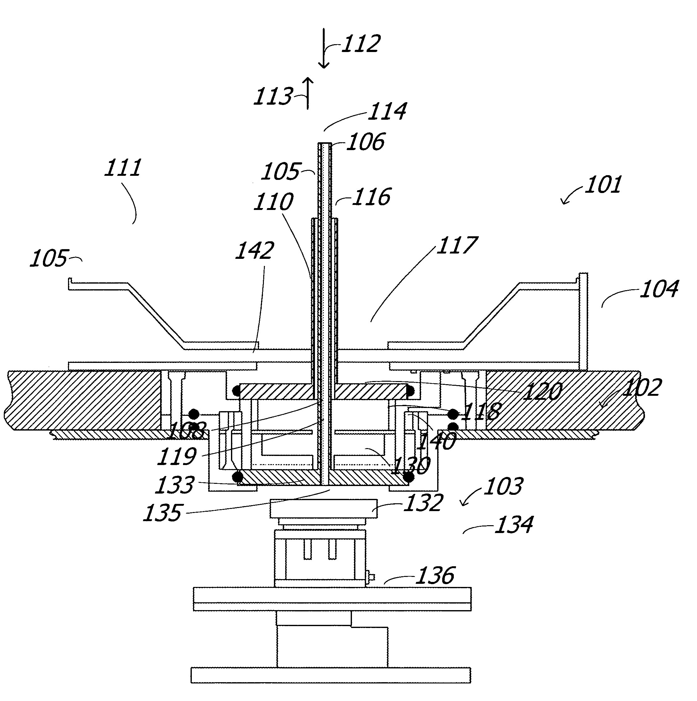
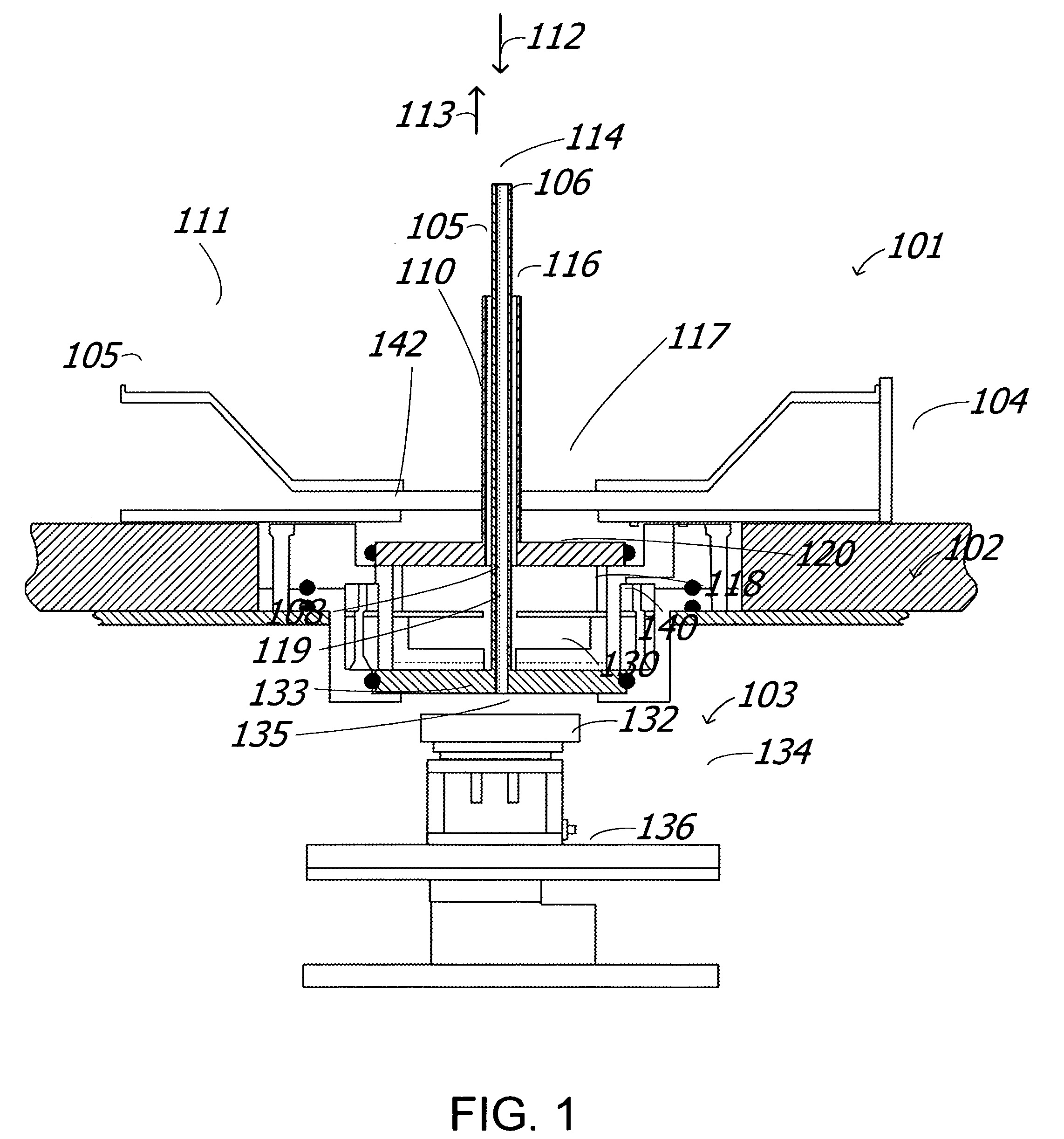
[0023]FIG. 1 illustrates a ...


PUM

PropertyMeasurementUnit
frequenciesaaaaaaaaaa
linear velocityaaaaaaaaaa

Abstract

A system and method for removing photoresist or other organic compounds from semiconductor wafers is provided. Non-fluorinated reactant gases (O2, H2, H2O, N2 etc.) are activated in a quartz tube by a medium pressure surface wave discharge. As the plasma jet impinges on a substrate, volatile reaction products (H2O, CO2, or low molecular weight hydrocarbons) selectively remove the photoresist from the surface. The medium pressure also enables high gas temperatures that provide an effective source of heat in the reactive zone on the wafer that enhances etch rates and provides a practical means of removing ion implanted photoresist.

Description

CROSS REFERENCE TO RELATED APPLICATIONS [0001] The present invention claims priority under 35 U.S.C. §119(e) to U.S. Provisional Application No. 60 / 633,673 filed on Dec. 6, 2004.TECHNICAL FIELD [0002] The present invention relates in general to semiconductor processing, and in particular, to the selective removal of surface layers from a workpiece, as for example, a semiconductor wafer in the manufacture of integrated circuits. It will be understood that while the following discussion is directed to semiconductor manufacturing proceses, the present invention may apply to various manufacturing processes and apparatus therefore such that the present invention shall not be limited to semiconductor manufacturing. BACKGROUND INFORMATION [0003] Photoresist masks define every layer of an integrated circuit (IC), from front-end-of-line (FEOL) ion implantation for isolation, P-or N-well doping, threshold voltage adjustment and source-drain contacts to back-end-of-line (BEOL) plasma etching o...

Claims


Application Information

Patent Timeline
Patent Type & Authority Applications(United States)
IPC IPC(8): C23F1/00
CPCG03F7/427H01J37/32357H01L21/67069H01L21/31138H01J37/32376
Inventor WOLFE, JOHN C.SRIVASTAVA, ASEEM K.BERRY, IVAN I.SAKTHIVEL, PALANIKUMARAN
Owner UNIV HOUSTON SYST
Why Eureka
Try Eureka