Micro LED light-emitting display array pixel unit structure and fabrication method thereof

A light-emitting display and pixel unit technology, applied in electrical components, electric solid-state devices, circuits, etc., can solve the problems of low reliability, unfavorable high-density integration of display devices, complex processes, etc., to improve integration density and reliability, high Quality display effect, save the effect of complicated process

Inactive Publication Date: 2018-05-08
GUANGDONG INST OF SEMICON IND TECH
View PDF4 Cites 14 Cited by
  • Summary
  • Abstract
  • Description
  • Claims
  • Application Information

AI Technical Summary

Problems solved by technology

However, the above method has the following problems: (1) The display array contains hundreds of thousands to millions of pixels, each pixel needs at least one solder joint, and the entire display array requires many solder joints, and the distance between the solder joints is small, so The process is complicated and the reliability is low, which is not conducive to industrial production; (2) The active drive display array is made by welding technology, and each pixel needs to be welded. In order to ensure the reliability of the device, a certain distance must be maintained between the solder points. Not conducive to high-density integration of display devices

Method used


Image

  • Micro LED light-emitting display array pixel unit structure and fabrication method thereof
  • Micro LED light-emitting display array pixel unit structure and fabrication method thereof
  • Micro LED light-emitting display array pixel unit structure and fabrication method thereof

Examples


Embodiment 1

[0075] This embodiment provides a method for manufacturing a pixel unit structure of a micro-LED light-emitting display array, the method comprising the following steps:

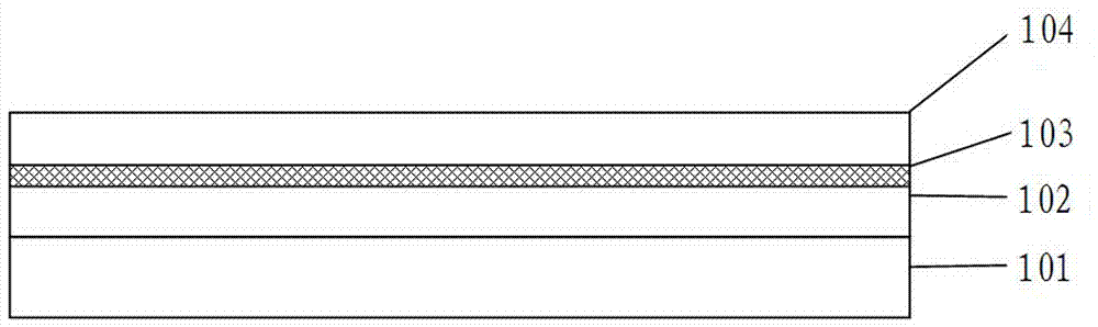
[0076] In step S101, a substrate 101 is provided, and an N-type semiconductor layer 102, an active region layer 103, and a P-type semiconductor layer 104 for forming an epitaxial wafer are sequentially grown upward on the substrate 101, as shown in 2;

[0077] In this embodiment, the substrate may be any material substrate among sapphire, diamond, silicon, gallium arsenide, silicon carbide, and gallium nitride. The growth of the N-type semiconductor layer 102 , the active region layer 103 and the P-type semiconductor layer 104 is realized by MOCVD (Metal Organic Compound Chemical Vapor Deposition) equipment. The material of the semiconductor layer includes but not limited to GaAs, AlGaInP, AlInP, AlGaAs, InGaP, GaP, GaN, InGaN, AlGaN and other materials;

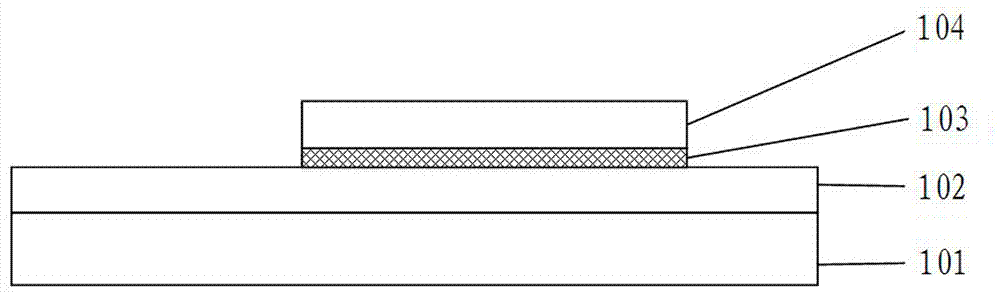
[0078] Step S102, using photolithography and etchin...

Embodiment 2

[0098] This embodiment provides another manufacturing method of a pixel unit structure of a micro-LED light-emitting display array, and the method includes the following steps:

[0099] Step S201 to step S204 are the same as step S101 to step S104 in the first implementation example.

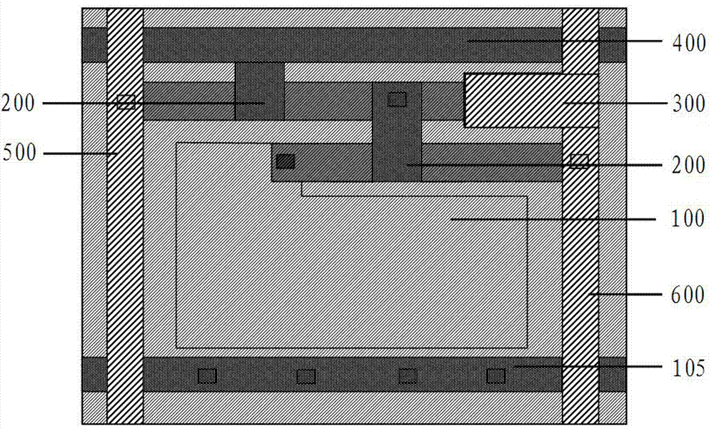
[0100] Step S205, depositing a film with good conductivity on the side where the insulating passivation film is deposited is used to prepare the gate electrode 205 of the thin film transistor, the N electrode 105 of the light emitting diode, the negative electrode 301 of the plate capacitor and the signal line 400, such as Figure 14 shown;

[0101] In this embodiment, the material of the thin film with good conductivity can be metal such as Ti, Ni, Au, Al, Cr, Mo, Pt, Ge, or one or more of oxides such as ITO. The manufacturing method of the ohmic contact electrode thin film can be evaporation or sputtering, and can be realized by etching or stripping process.

[0102] Step S206, depositing a ...


PUM


Abstract

The invention relates to a micro LED light-emitting display array pixel unit structure and a fabrication method thereof. The micro LED light-emitting display array pixel unit structure comprises a display pixel unit body, wherein the display pixel unit body comprises a light-emitting diode, a light-emitting diode driving circuit and a lead, wherein the light-emitting diode is manufactured by integration of an epitaxial wafer grown on a substrate, and the lead is used for connecting the outside. Three parts required by manufacturing of the display pixel unit are integrated with the epitaxial wafer by a semiconductor processing technology, the pixel light-emitting unit and the control circuit are integrated, so that the welding process with complicated process and low reliability is omitted,the fabrication process is simple, and active driving of a micro LED display array can be achieved without independently fabricating a pixel driving circuit; and moreover, the integration density andthe reliability of the micro LED display array are effectively improved, the display effect with high-speed scanning, high definition and high quality can be achieved, the demand of next-generation display application is satisfied, and industrialization is promoted.

Description

technical field [0001] The invention relates to the technical field of micro-LED light-emitting display arrays, in particular to a micro-LED light-emitting display array pixel unit structure and a manufacturing method thereof. Background technique [0002] In recent years, with the development of epitaxial materials and LED (light-emitting diode) chip technology, it has become possible to use LEDs as micro-LED display arrays for light-emitting unit pixels. Micro LED display is an all-solid-state light-emitting array that integrates a high-density two-dimensional light-emitting diode array on a substrate. Micro LED display array devices have the advantages of self-illumination, high brightness, long life, and fast response speed, and have great market potential. Micro LED light-emitting display arrays can be divided into passive drive arrays and active drive arrays according to different driving methods. Generally, the manufacturing method of actively driving display arrays ...

Claims


Application Information

Patent Timeline
Patent Type & Authority Applications(China)
IPC IPC(8): H01L27/15H01L33/00
CPCH01L27/156H01L33/005
Inventor 刘久澄龚政潘章旭陈志涛刘晓燕任远曾昭烩李叶林
Owner GUANGDONG INST OF SEMICON IND TECH
Why Eureka
Try Eureka