Electron beam lithography method

Inactive Publication Date: 2006-10-31
SAMSUNG ELECTRONICS CO LTD
View PDF3 Cites 34 Cited by
  • Summary
  • Abstract
  • Description
  • Claims
  • Application Information

AI Technical Summary

Benefits of technology

[0021]According to the present invention, it is possible to minimize butting errors occurring at a boundary between stripes, so as to minimize the time necessary for exposure p

Problems solved by technology

When a mask is fabricated using the electron beam, the size of the electron beam is limited to a very small region, and so it is difficult to expose the whole mask.
When the stripes or frames are sequentially exposed to the electron beam, a so-called butting error, i.e. wrenching between adjacent stripes, occurs.
The butting error represents an error in which a pattern ranging over an interval between the stripes, which is transferred by the exposure, is wrenched or dropped from the stripe boundary.
Because of the butting error, a critical dimension error in which the critical dime

Method used


Image

  • Electron beam lithography method
  • Electron beam lithography method
  • Electron beam lithography method

Examples


Embodiment Construction

[0028]The present invention now will be described more fully with reference to the accompanying drawings, in which preferred embodiments of the invention are shown. This invention may, however, be embodied in many different forms and should not be construed as being limited to the embodiments set forth herein; rather, these embodiments are provided so that this disclosure will be thorough and complete and will fully convey the concept of the invention to those skilled in the art. In the drawings, the shapes of elements are exaggerated for clarity, and like reference numerals are used to refer to like elements throughout the application.

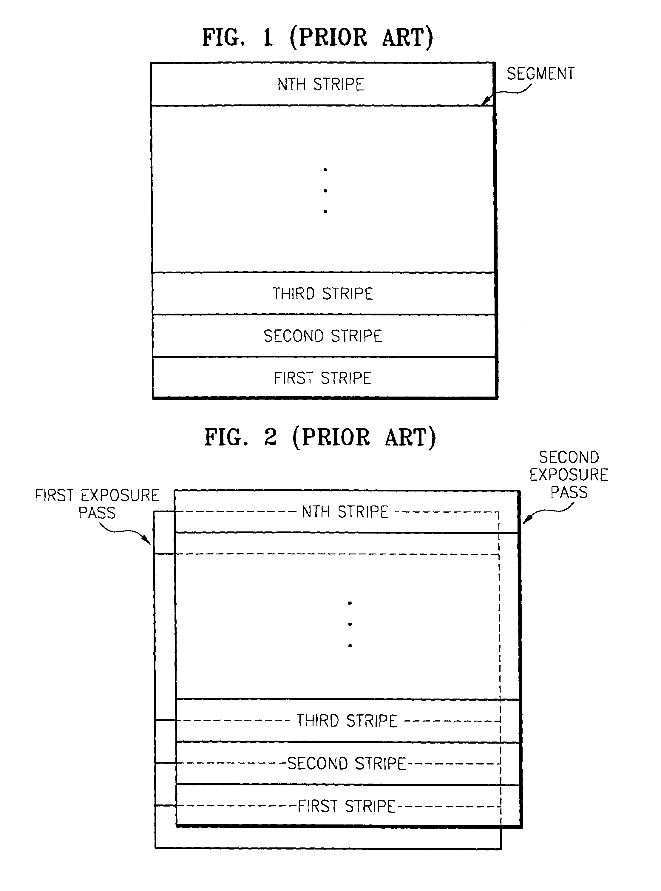
[0029]In preferred embodiments of the present invention, electron beam exposure is performed by setting boundaries of stripes to overlap with boundaries of adjacent stripes. Such stripes tend to be wider than a conventional stripe shown in FIG. 1.

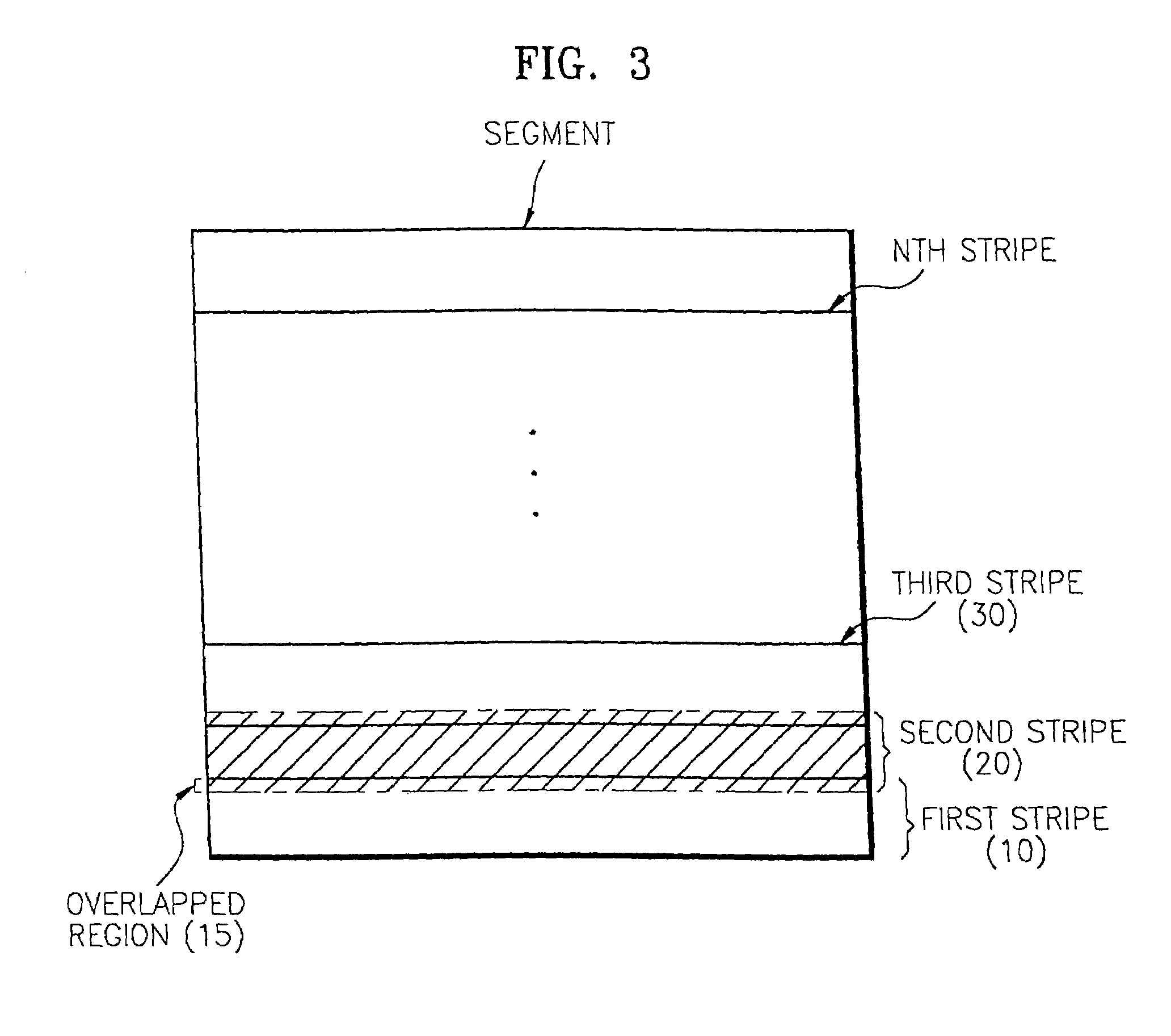
[0030]FIG. 3 is a schematic diagram for explaining a method of performing electron beam lithography accord...


PUM


Abstract

An electron beam lithography method includes extending the widths of a plurality of stripes which divide a region where an electron beam exposure is to be performed, so that the boundaries of the stripes overlap adjacent stripes at each boundary, and sequentially exposing each of the stripes to an electron beam.

Description

BACKGROUND OF THE INVENTION[0001]1. Field of the Invention[0002]The present invention relates to manufacturing a semiconductor device, and more particularly, to a method of electron beam lithography for minimizing throughput loss and preventing butting errors from occurring.[0003]A claim of priority is made to Korean Patent Application No. 2002-0047230, filed Aug. 9, 2002, the contents of which are incorporated herein by reference.[0004]2. Description of the Related Art[0005]Among semiconductor fabricating processes, a lithography process using an electron beam is used to transfer a delicate pattern. Until now, lithography using a electron beam has generally been used for fabricating a photo mask in which printing a delicate pattern is regarded as a very important factor.[0006]When a mask is fabricated using the electron beam, the size of the electron beam is limited to a very small region, and so it is difficult to expose the whole mask. Therefore, electron beam lithography equipme...

Claims


Application Information

Patent Timeline
IPC IPC(8): G03C5/00G03F7/22G03F7/20H01J37/317
CPCB82Y10/00B82Y40/00G03F7/2059H01J37/3174Y10S430/143G03F7/22
Inventor KI, WON-TAI
Owner SAMSUNG ELECTRONICS CO LTD
Why Eureka
Try Eureka