

Method of growing semiconductor nanowires with uniform cross-sectional area using chemical vapor deposition
a technology of chemical vapor deposition and semiconductor nanowires, which is applied in the direction of nanoinformatics, crystal growth process, polycrystalline material growth, etc., can solve the problems of non-uniform cross-sectional area, significant taper of nanowires, and unsuitability for us
- Summary
- Abstract
- Description
- Claims
- Application Information
AI Technical Summary
Benefits of technology
Problems solved by technology
Method used
Image

Examples
Embodiment Construction
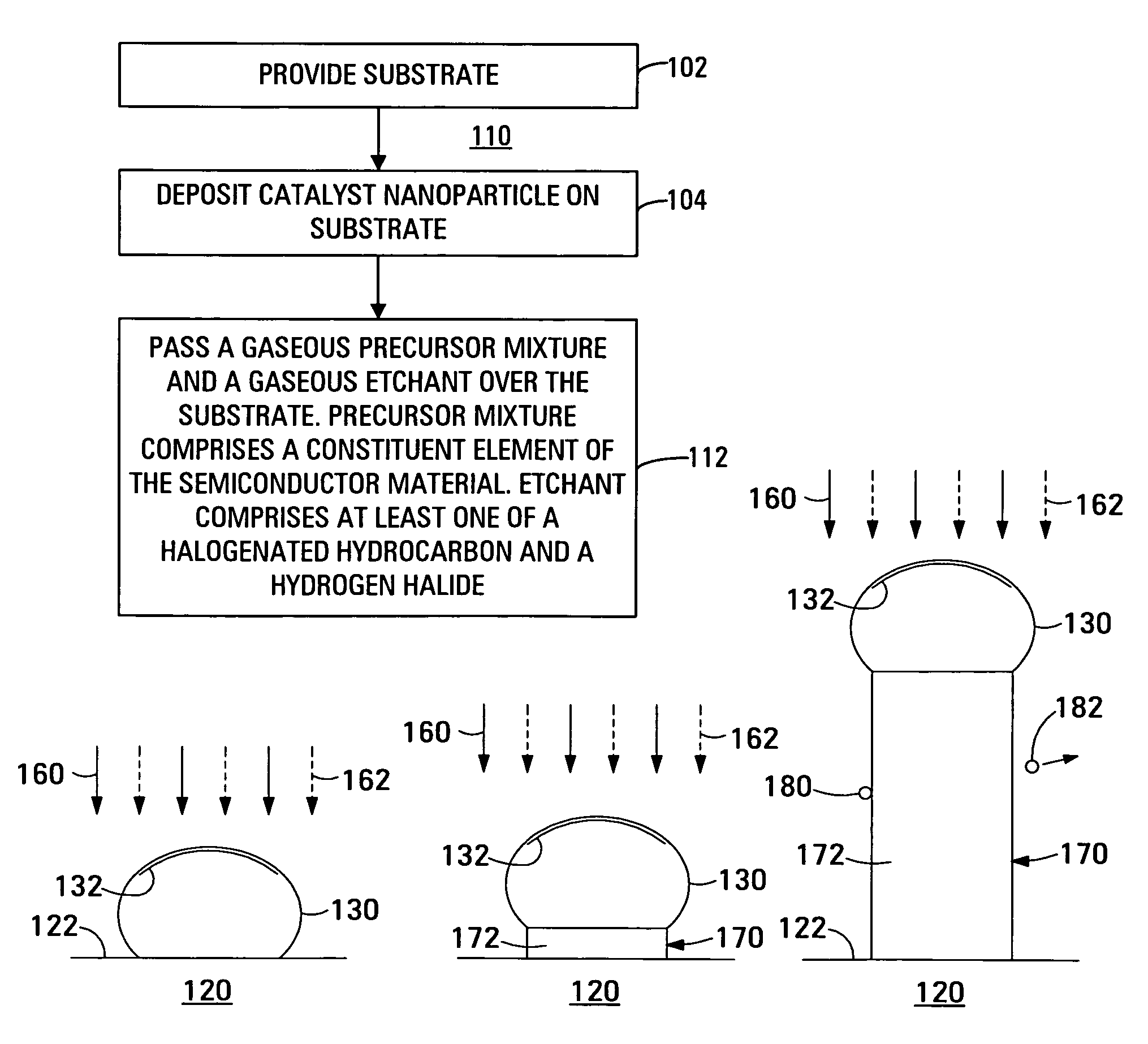
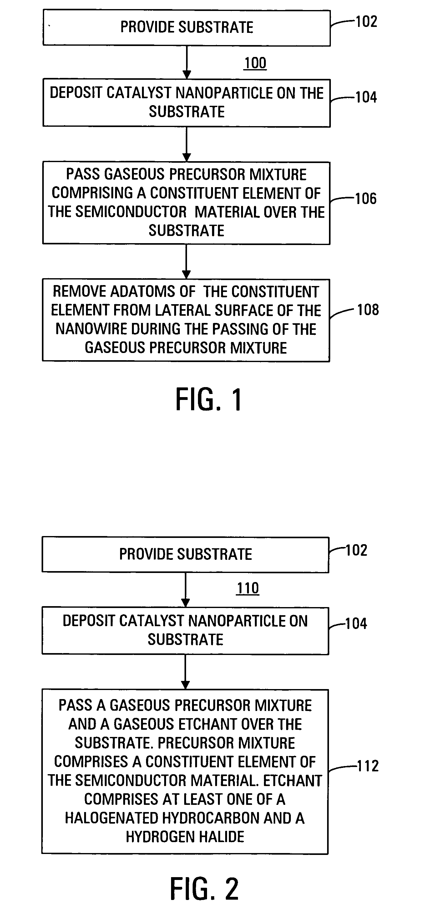
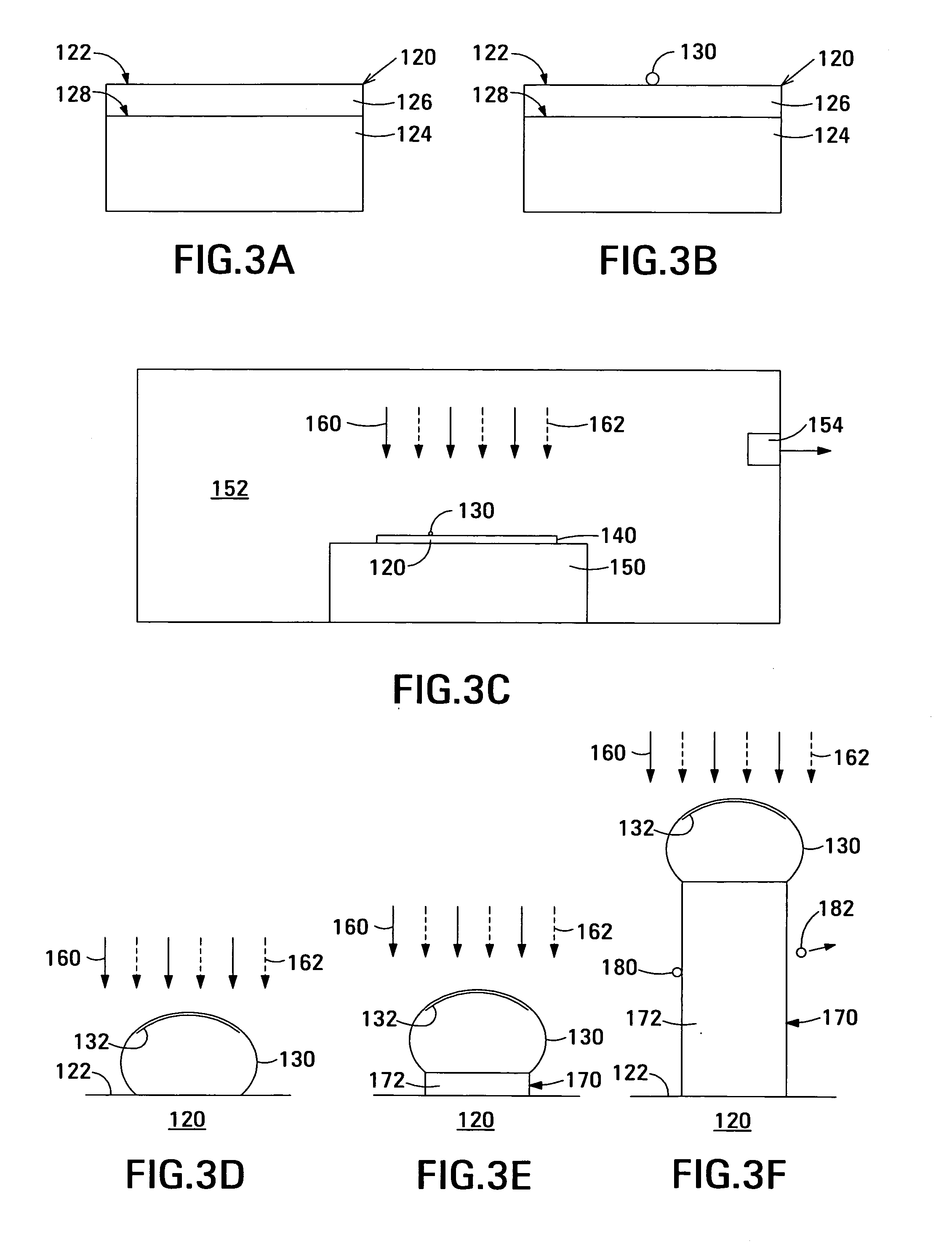
[0018]FIG. 1 is a flow chart illustrating a first embodiment 100 of a method in accordance with the invention for using a chemical vapor deposition (CVD) process such as metal-organic chemical vapor deposition (MOCVD) to grow a nanowire of a semiconductor material. The nanowire has a uniform cross-sectional area along its length.
[0019]In block 102, a substrate is provided.
[0020]In block 104, a catalyst nanoparticle is deposited on the substrate.
[0021]In block 106, a gaseous precursor mixture comprising a constituent element of the semiconductor material of the nanowire is passed over the substrate.
[0022]In block 108, adatoms of the constituent element are removed from a lateral surface of the nanowire during the passing of the precursor mixture.
[0023]In an embodiment, in block 108, the adatoms of the constituent element are removed by additionally passing a gaseous etchant over the substrate.
[0024]In another embodiment, in block 108, the adatoms of the constituent element are remove...
PUM
| Property | Measurement | Unit |
|---|---|---|
| diameter | aaaaa | aaaaa |
| temperature | aaaaa | aaaaa |
| melting point | aaaaa | aaaaa |
Abstract
Description
Claims
Application Information