This helps you quickly interpret patents by identifying the three key elements:
Problems solved by technology
Method used
Benefits of technology
Benefits of technology
[0062]By the above structure, in the light-emitting device of the present invention, the number of thin film transistors provided in each of pixels is made two to prevent a drop in an opening ratio, and it becomes possible to suppress uneven luminance due to fluctuation in the threshold voltage of the current controlling TFT included in each of the pixels.
[0069]By the above structure, in the light-emitting device of the present invention, the number of thin film transistors provided in each of the pixels is made two to prevent a drop in the opening ratio, and it becomes possible to suppress uneven luminance due to fluctuation in threshold voltage of current controlling TFTs included in the respective pixels.
[0076]By the above structure, in the light-emitting device of the present invention, the number of thin film transistors provided in each of pixels is made two to suppress a drop in the opening ratio, and it becomes possible to suppress uneven luminance due to fluctuation in threshold voltage of current controlling TFTs included in the respective pixels.
Problems solved by technology
Besides, if the number of TFTs provided in a pixel is increased, there is a fear that yield of the light-emitting device itself is lowered.
Method used
Image
Click on the blue label to locate the original text in one second.
Reading with bidirectional positioning of images and text.
Examples
embodiment 1
[0166]In this embodiment, an example in which the present invention is applied to an actual light-emitting device by using the above described expressions 8 and 11 will be described.
[0167]In this embodiment, a light-emitting device having a resolution of QVGA of 320×240 and a size of 4 inches will be exemplified.
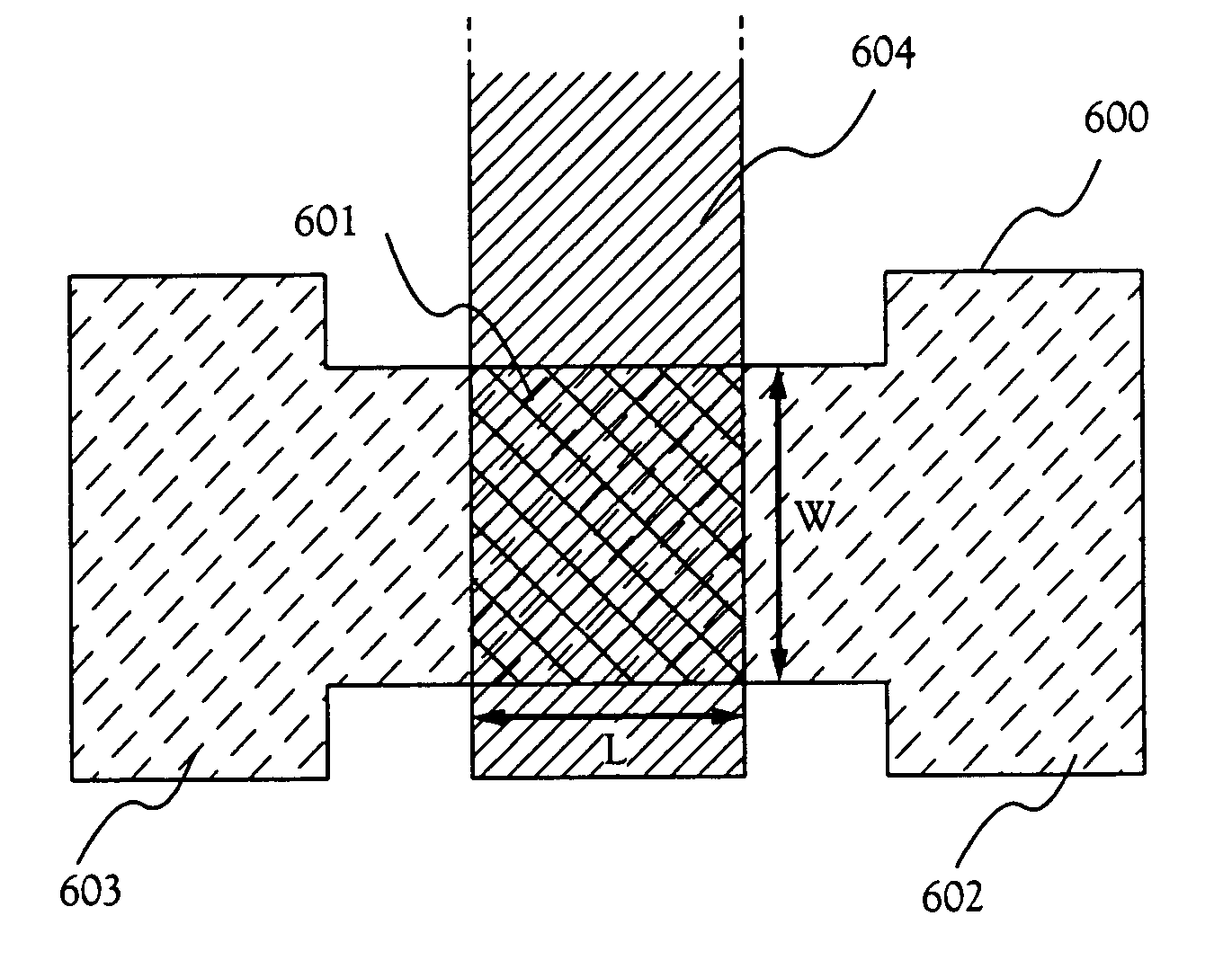
[0168]A pixel size of the 4-inch QVGA light-emitting device is about 84 μm×252 μm. When an attempt to obtain definite luminance is made, the intensity of current flowing through an EL element per unit area is determined. In this embodiment, it is made 3 mA / cm2 per unit area.
[0169]Thus, a drain current Id of a current controlling TFT included in each of pixels is expressed by the following expression 22.
Id=3*(84*10−4)*(252*10−4)=6.35*1031 7 A [Expression 22]
[0170]The above expression indicates a value of the drain current Id of the current controlling TFT when the opening ratio of the light-emitting device is 100%. Actually, in almost all cases, the opening ratio of the ligh...
embodiment 2
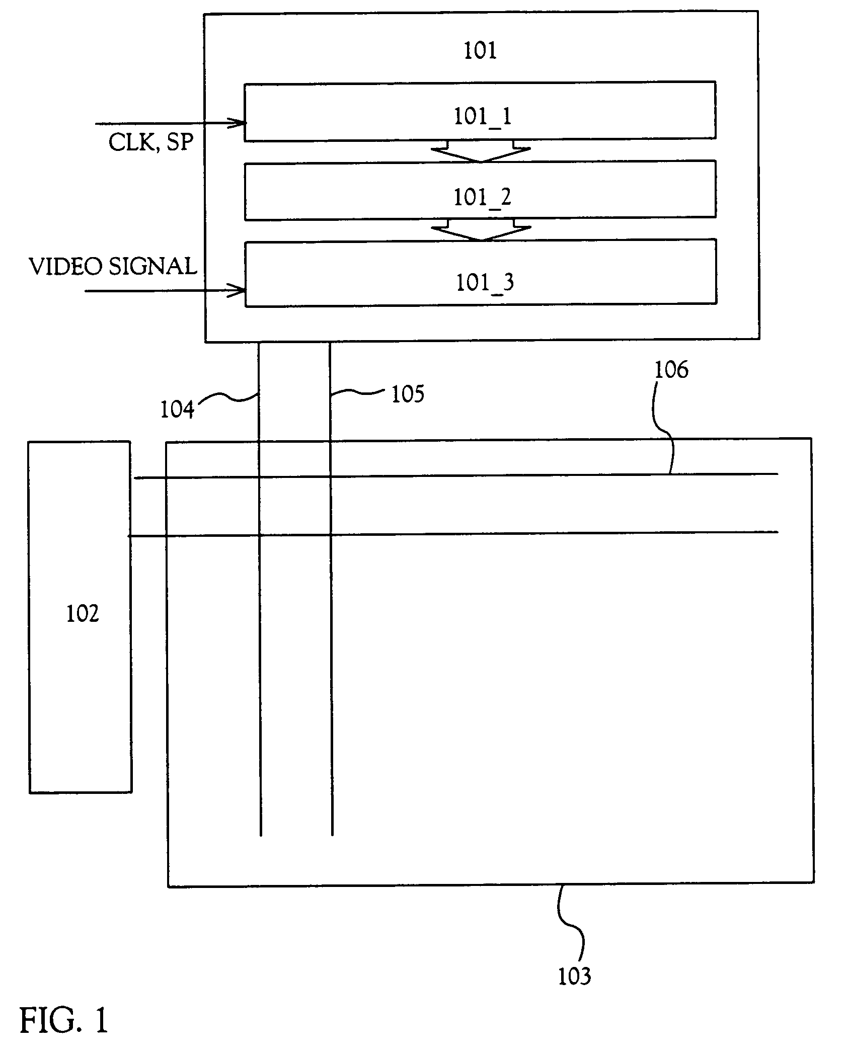
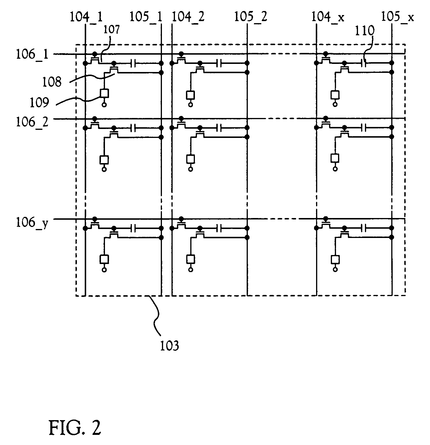
[0183]A driving method of a light-emitting device of the present invention will be described with reference to FIGS. 1 to 3.
[0184]FIG. 1 is a top view of a light-emitting device of the present invention. Reference numeral 101 designates a source signal line driving circuit; 102, a gate signal line driving circuit; and 103, a pixel portion. In this embodiment, although one source signal line driving circuit and one gate signal line driving circuit are provided, the present invention is not limited to this structure. Two source signal line driving circuits may be provided, or two gate signal line driving circuits may be provided.
[0185]The source signal line driving circuit 101 includes a shift register 101_1, a level shift 101_2, and a sampling circuit 101_3. Note that the level shift 101_2 has only to be used as the need arises, and it may not be always used. Besides, although this embodiment is made to have such a structure that the level shift 101_2 is provided between the shift re...
embodiment 3
[0202]In this embodiment, a detailed description will be given of a method of fabricating a pixel portion and TFTs (n-channel TFT and p-channel TFT) of a driving circuit provided on the periphery of the pixel portion on the same substrate at the same time.
[0203]First, as shown in FIG. 7A, an under film 701 made of an insulating film such as a siliconoxide film, a siliconnitride film, or a siliconnitrideoxide film is formed on a substrate 700 made of glass such as bariumborosilicate glass or alumino borosilicate glass, typified by #7059 glass or #1737 glass of Corning Inc. For example, a silicon nitrideoxide film 701a fabricated from SiH4, NH3 and N2O by a plasma CVD method is formed to a thickness of 10 to 200 nm (preferably 50 to 100 nm), and a hydrogenated silicon nitride oxide film 701b similarly fabricated from SiH4 and N2O is formed to a thickness of 50 to 200 nm (preferably 100 to 150 nm) to form a laminate. In this embodiment, although the under film 701 is shown as the...
PUM
Abstract
There is provided an EL light-emitting device with less uneven brightness. When a drain current of a plurality of current controlling TFTs is Id, a mobility is μ, a gate capacitance per unit area is Co, a maximum gate voltage is Vgs(max), a channel width is W, a channel length is L, an average value of a threshold voltage is Vth, a deviation from the average value of the threshold voltage is ΔVth, and a difference in emission brightness of a plurality of EL elements is within a range of ±n %, a semiconductordisplay device is characterized in thatA=2Idμ*C0A(Vgs(max)-Vth)2≦WL≦(1+n100-1)2*AΔVth2ΔVth≦(1+n100-1)*A*L / W
Description
CROSS-REFERENCE TO RELATED APPLICATIONS[0001]This application is a divisional application of U.S. application Ser. No. 09 / 796,412, filed on Feb. 27, 2001 now U.S. Pat. No. 6,583,776, which claims the benefit of a foreign priority application filed in Japan, Ser. No. 2000-054963, filed Feb. 29, 2000, all of which are incorporated by reference.BACKGROUND OF THE INVENTION[0002]1. Field of the Invention[0003]The present invention relates to an EL panel in which an EL element formed on a substrate is sealed between the substrate and a cover member. Further, the present invention relates to an EL module in which an IC is mounted in the EL panel. Incidentally, in the present specification, the EL panel and the EL module are generally referred to as a light-emitting device. The present invention further relates to an electronic instrument using the light-emitting device.[0004]2. Description of the Related Art[0005]In recent years, a technique for forming a TFT on a substrate has been greatl...
Claims
Application Information
Patent Timeline
Application Date:The date an application was filed.
Publication Date:The date a patent or application was officially published.
First Publication Date:The earliest publication date of a patent with the same application number.
Issue Date:Publication date of the patent grant document.
PCT Entry Date:The Entry date of PCT National Phase.
Estimated Expiry Date:The statutory expiry date of a patent right according to the Patent Law, and it is the longest term of protection that the patent right can achieve without the termination of the patent right due to other reasons(Term extension factor has been taken into account ).
Invalid Date:Actual expiry date is based on effective date or publication date of legal transaction data of invalid patent.

