Semiconductor integrated circuit device and device for testing same

Inactive Publication Date: 2006-10-31
RENESAS ELECTRONICS CORP
View PDF7 Cites 8 Cited by
  • Summary
  • Abstract
  • Description
  • Claims
  • Application Information

AI Technical Summary

Benefits of technology

[0012]It is therefore an object of the present invention to provide a semiconductor integrated circuit device which can inexpensiv

Problems solved by technology

Semiconductor integrated circuit devices (hereinafter referred to as “LSI chips”), recently available in larger scale integration and higher densities, which are not designed for an easy testing configuration, cannot be tested and diagnosed for faults.
The conventional LSI chip testing process is problematic in that since a frequency which can be used in the delay test depends on

Method used


Image

  • Semiconductor integrated circuit device and device for testing same
  • Semiconductor integrated circuit device and device for testing same
  • Semiconductor integrated circuit device and device for testing same

Examples


1st embodiment

[0036

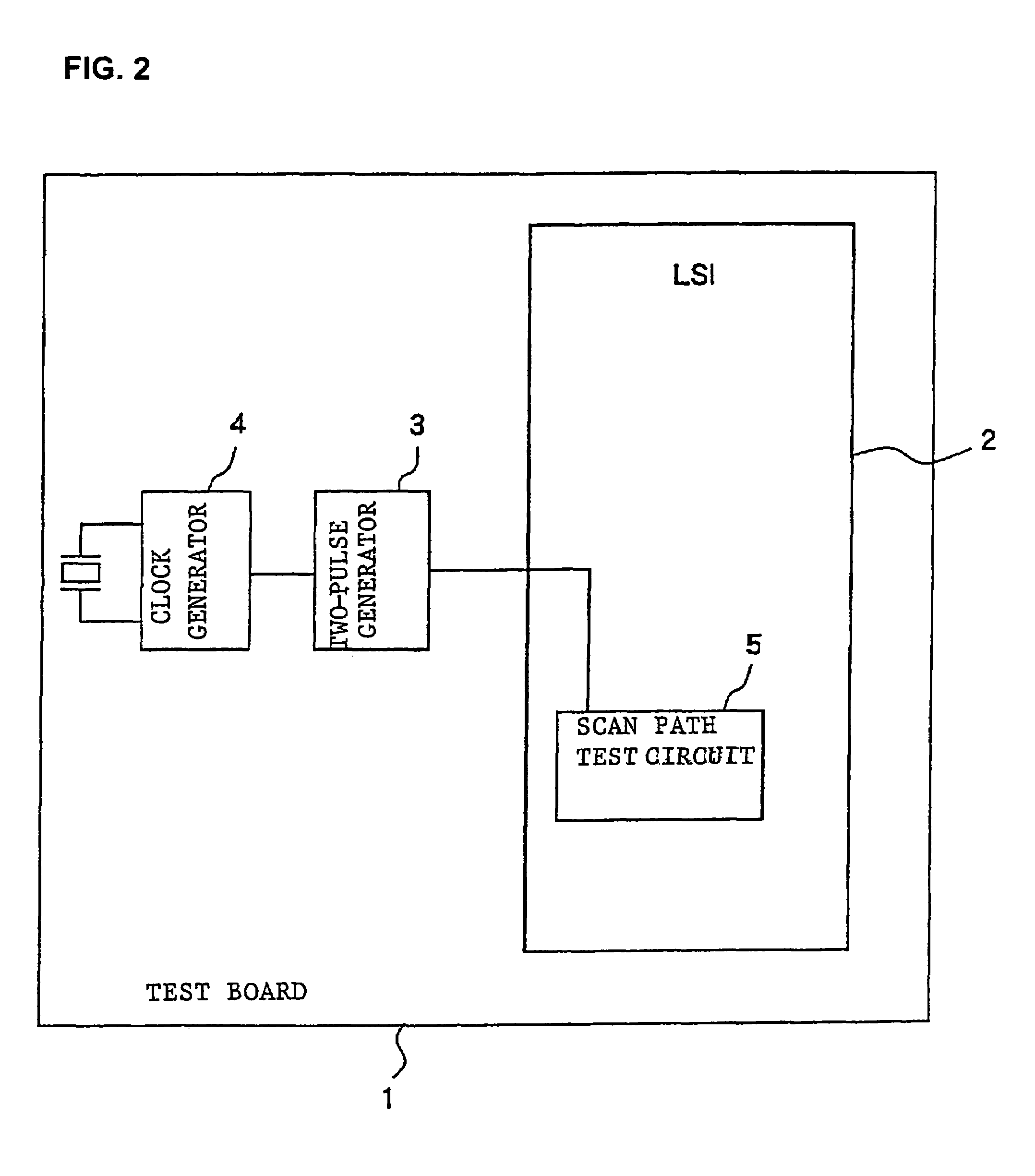
[0037]FIG. 2 shows in block form a device for testing a semiconductor integrated circuit device according to a first embodiment of the present invention. FIG. 3 shows a two-pulse generator in the device shown in FIG. 2, and FIG. 4 shows the manner in which the two-pulse generator shown in FIG. 3 operates.

[0038]As shown in FIG. 2, the device for testing a semiconductor integrated circuit device according to a first embodiment of the present invention has test board 1 on which LSI chip 2 to be tested is removably placed, two-pulse generator 3 mounted on test board 1 for generating two pulses for a delay test which are to be supplied to LSI chip 2, and clock generator 4 mounted on test board 1 for generating a test clock for operating two-pulse generator 3 at a suitable timing.

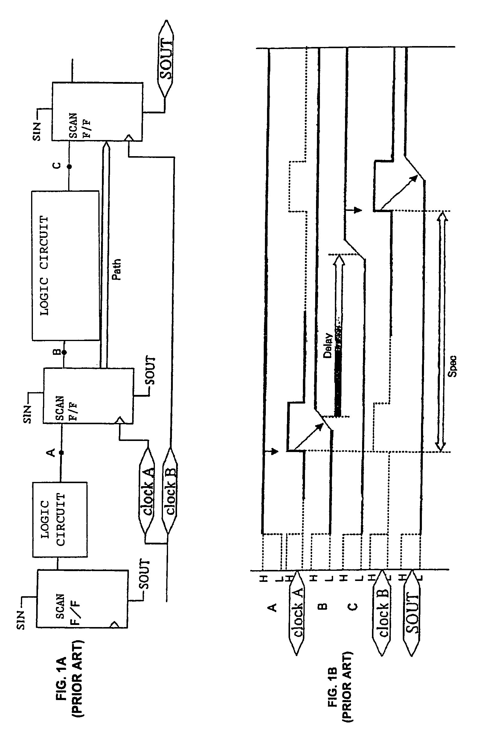
[0039]Clock generator 4 generates a test clock having a frequency for use in a delay test. Two-pulse generator 3 extracts two pulses from the test block in timed relation to a control pulse input from an ext...

2nd embodiment

[0048

[0049]FIG. 5 shows in block form a device for testing a semiconductor integrated circuit device according to a second embodiment of the present invention.

[0050]As shown in FIG. 5, the testing device according to the second embodiment differs from the testing device according to the first embodiment in that two-pulse generator 13 which is identical to the two-pulse generator according to the first embodiment is incorporated in LSI 12 to be tested. The testing device according to the second embodiment has clock generator 14 which is identical to the clock generator according to the first embodiment. Therefore, details of clock generator 14 will not be described below.

[0051]With two-pulse generator 13 being incorporated in LSI chip 12, LSI chip 12 can be put to a delay test simply by supplying a test clock having a predetermined frequency from clock generator 14 or a general-purpose oscillator or a tester to the test board.

3rd embodiment

[0052

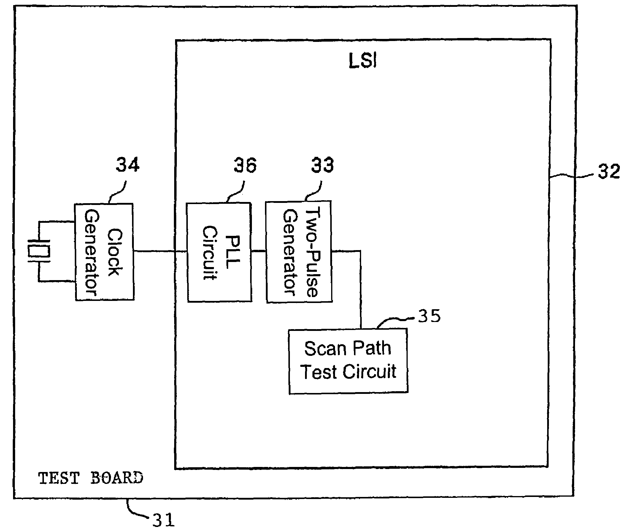
[0053]FIG. 6 shows in block form a device for testing a semiconductor integrated circuit device according to a third embodiment of the present invention.

[0054]As shown in FIG. 6, the testing device according to the third embodiment differs from the testing device according to the first embodiment in that PLL (Phase-Locked Loop) circuit 26 for multiplying the frequency of the test clock output from clock generator 24 and supplying a signal having the multiplied-frequency signal to two-pulse generator 23 is additionally mounted on test board 21. PLL circuit 26 may comprise a phase comparator, a VCO (Voltage-Controlled Oscillator), a loop filter, and a frequency divider, which are of known nature. Two-pulse generator 23 and clock generator 24 are identical to those according to the first embodiment, and will not be described in detail below.

[0055]In the third embodiment, since the frequency of the test clock output from clock generator 24 is multiplied by PLL circuit 26, the frequ...


PUM


Abstract

A device for testing a semiconductor integrated circuit device has a test board on which the semiconductor integrated circuit device to be tested is removably mounted, and a two-pulse generator mounted on the test board, for generating two pulses spaced from each other by a pulse interval equal to the period of a test clock for the delay test, from the test clock, and supplying the generated two pulses to the scan path test circuit. The device also has a PLL circuit for multiplying the frequency of the test clock and supplying a signal having the multiplied-frequency to the two-pulse generator.

Description

BACKGROUND OF INVENTION[0001]1. Field of the Invention[0002]The present invention relates to a semiconductor integrated circuit device and a device for testing such a semiconductor integrated circuit device, and more particularly to a semiconductor integrated circuit device suitable for a delay test using a scan path test circuit, and a device for testing such a semiconductor integrated circuit device.[0003]2. Description of the Related Art[0004]Semiconductor integrated circuit devices (hereinafter referred to as “LSI chips”), recently available in larger scale integration and higher densities, which are not designed for an easy testing configuration, cannot be tested and diagnosed for faults. One known approach for easy testing is a scan path process in which flip-flops in a semiconductor integrated circuit are connected into a chain pattern so as to operate as a shift register, and when the circuit is tested, the values of the flip-flops are controlled and observed from outside of...

Claims


Application Information

Patent Timeline
IPC IPC(8): G01R31/28G01R31/3185G01R31/319H01L21/822H01L27/04
CPCG01R31/318552G01R31/31917G01R31/31926
Inventor OZAKI, HIDEHARU
Owner RENESAS ELECTRONICS CORP
Why Eureka
Try Eureka