Fast and accurate optical proximity correction engine for incorporating long range flare effects

a long-range flare and optical proximity technology, applied in the field of optical lithography, can solve the problems of limiting the accuracy of predictions, complex opc methodologies, and high computational intensity of all models, and achieve the effect of reasonable accuracy and reduced tim

Active Publication Date: 2006-10-31
GLOBALFOUNDRIES U S INC
View PDF4 Cites 15 Cited by
  • Summary
  • Abstract
  • Description
  • Claims
  • Application Information

AI Technical Summary

Benefits of technology

[0041]It is yet another object of the present invention to reduce the time needed to simulate the flare effect.
[0042]It is a more particular object of the present invention to provide a reasonably accurate solution for the flare effect simulation.

Problems solved by technology

However, the ever shrinking device dimensions combined with the desire to enhance circuit performance in the deep sub-wavelength domain require complex OPC methodologies to ensure the fidelity of mask patterns on the printed wafer.
Since present lithographic tools employ partially coherent illumination, such modeling is computationally intensive for all but the most elementary patterns.
In prior art MBOPC tools, the physical effects simulated include only the diffraction of light in the presence of low order aberrations which limit the accuracy of the predictions.
The problem is even more pronounced in bright field masks that are used in printing critical levels which control the ultimate performance of the circuit, such as gate and diffusion levels.
A significant difficulty when taking into consideration long range effects, such as flare, is the extent of the corrections flare effects required on the mask.
Current Model-Based OPC (MBOPC) software tools are not equipped to handle such long distance effects.
The non-optimal interferometer grossly underestimates the energy of the flare.
Any increase in size of that region significantly affects the timing and accuracy of the simulation and, consequently, affects the OPC results.
Second, even when the power spectrum of the wavefront is known or inferred, it is not possible to include the effect of high frequency wavefront components on an image integral that is truncated at a short ROI distance, causing most of the scattered light to be neglected.
Finally, it is not straightforward to include these terms in the calculated image.
As a result, ordinary interferometric instruments will not detect it.
Currently there are no tools available for Model-Based Optical Proximity Correction (MBOPC) incorporating flare effects and there are no known patents or publications available to that effect.

Method used


Image

  • Fast and accurate optical proximity correction engine for incorporating long range flare effects
  • Fast and accurate optical proximity correction engine for incorporating long range flare effects
  • Fast and accurate optical proximity correction engine for incorporating long range flare effects

Examples


Embodiment Construction

[0064]In describing the preferred embodiment of the present invention, reference will be made herein to FIGS. 6–8, in which like numerals refer to like features of the invention.

[0065]The present invention is ultimately used in optical lithography to correct for any distortions on a photo-mask having circuit patterns, in order to achieve an accurate projection thereof on the photo-resist coated wafers. In so doing, the invention provides model-based optical lithography simulations that incorporate long-range flare and stray-light effects when simulating a wafer image.

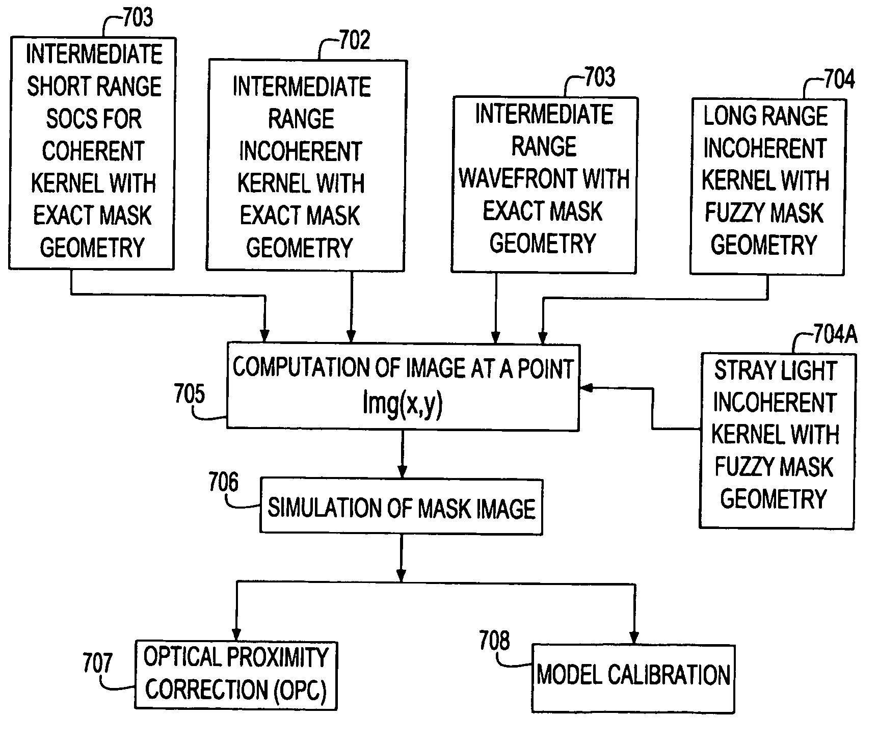
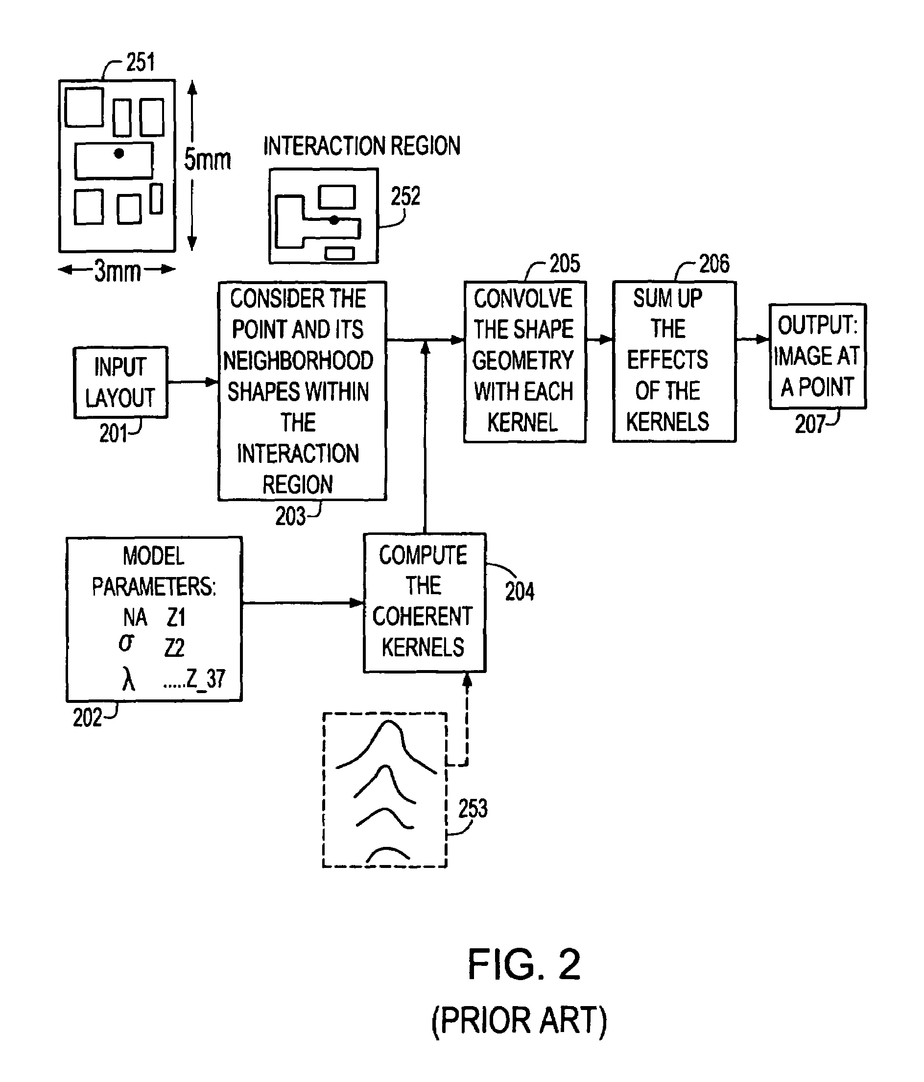
[0066]The present invention provide a significant improvement beyond the prior art, as illustrated in FIG. 2, for the computation of the image intensity at a point. In order to compute this image intensity, the invention considers the effect of flare emanating from all the shapes on the mask as opposed to a small region considered in the prior art.

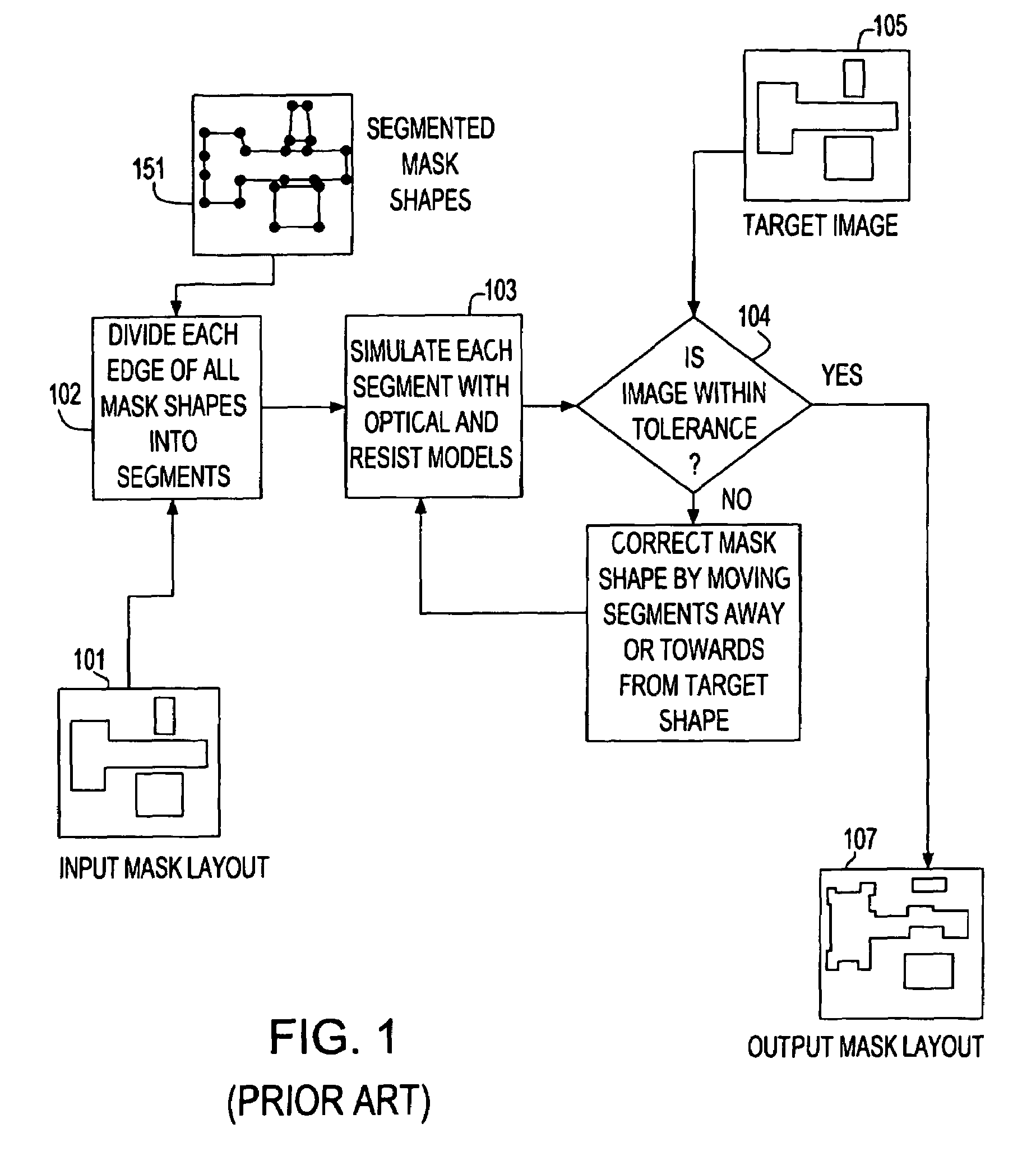
[0067]Whereas the prior art shown in FIG. 2 considers only short range in...


PUM

PropertyMeasurementUnit
reflectivityaaaaaaaaaa
distanceaaaaaaaaaa
distanceaaaaaaaaaa

Abstract

A method is described for performing model-based optical proximity corrections on a mask layout used in an optical lithography process having a plurality of mask shapes. Model-based optical proximity correction is performed by computing the image intensity on selected evaluation points on the mask layout. The image intensity to be computed includes optical flare and stray light effects due to the interactions between the shapes on the mask layout. The computation of the image intensity involves sub-dividing the mask layout into a plurality of regions, each region at an increasing distance from the evaluation point. The contributions of the optical flare and stray light effects due to mask shapes in each of the regions are then determined. Finally, all the contributions thus obtained are combined to obtain the final computation of the image intensity at the selected point.

Description

BACKGROUND OF THE INVENTION[0001]This invention relates generally to the field of optical lithography, and more particularly, to a method for incorporating long-range flare effects in an Optical Proximity Correction (OPC) software tool for use in a model-based optical lithography simulation, to provide a fast and accurate correction of the device shapes in a photo-mask.[0002]The optical micro-lithography process in semiconductor fabrication, also known as the photolithography process, consists of duplicating desired circuit patterns onto semiconductor wafers for an overall desired circuit performance. The desired circuit patterns are typically represented as opaque, complete and semi-transparent regions on a template commonly referred to as a photomask. In optical micro-lithography, patterns on the photo-mask template are projected onto the photo-resist coated wafer by way of optical imaging through an exposure system.[0003]The continuous advancement of VLSI chip manufacturing techn...

Claims


Application Information

Patent Timeline
Patent Type & Authority Patents(United States)
IPC IPC(8): G06F17/50G03F1/14
CPCG03F1/144G03F1/36G03F1/70
Inventor GALLATIN, GREGG M.GOFMAN, EMANUELLAI, KAFAILAVIN, MARK A.RAMM, DOVROSENBLUTH, ALAN E.SHLAFMAN, SHLOMOCHEN, ZHENGMUKHERJEE, MAHARAJ
Owner GLOBALFOUNDRIES U S INC
Why Eureka
Try Eureka