Process for implementing conductive tracing layout in touch panel

a technology of conductive tracing and touch panel, which is applied in the direction of conductive pattern formation, instruments, transportation and packaging, etc., can solve the problem of hard to narrow down the margin of touch, and achieve the effect of narrowing down the tracing width

Active Publication Date: 2006-11-07
INNOLUX CORP
View PDF4 Cites 2 Cited by
  • Summary
  • Abstract
  • Description
  • Claims
  • Application Information

AI Technical Summary

Benefits of technology

[0009]An object of the present invention is to provide a process for implementing conductive tracing layout in a touch panel, in order to narrow down the tracing width.
[0010]Another object of the present invention is to provide a process for implementing conductive tracing layout in a touch panel, able to reduce signal loss during the signal transmission so as to allow the shortening of the line-to-line space between every two conductive traces.
[0011]A further object of the present invention is to provide a process for implementing conductive tracing layout in a touch panel, in order to narrow down the margins of the conductive tracing layout region.

Problems solved by technology

A cathode ray tube (CRT) monitor has been gradually replaced by a liquid crystal display (LCD) due to the disadvantages of heavy weight, bulky size, and electromagnetic radiation.
Since the above-mentioned conductive tracing layout on the touch panel is achieved in a printing manner that conductive paste is formed on the upper substrate and the lower substrate, there are likely to be some disadvantages as described as follow: (1) relatively large trace width, e.g. larger than 0.5 mm, is required; (2) relatively large line-to-line space, e.g. wider than 0.7 mm, is required due to possible signal loss during signal transmission; and (3) it is hard to narrow down the margins of touch panel, i.e. the distance between the inner and outer edges of the tracing layout region 10C, due to the consideration of adhesion capability of the conductive paste.

Method used


Image

  • Process for implementing conductive tracing layout in touch panel
  • Process for implementing conductive tracing layout in touch panel
  • Process for implementing conductive tracing layout in touch panel

Examples


Embodiment Construction

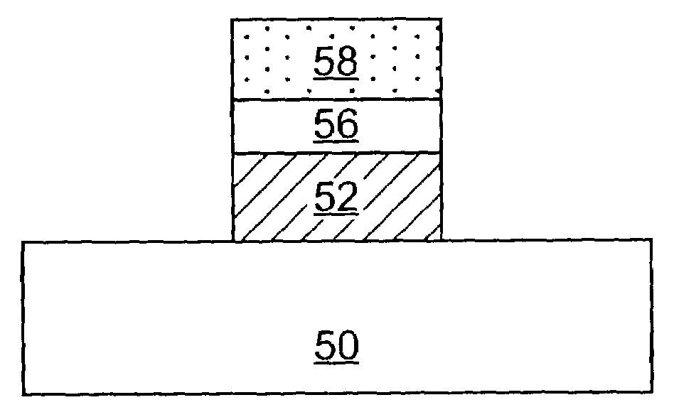
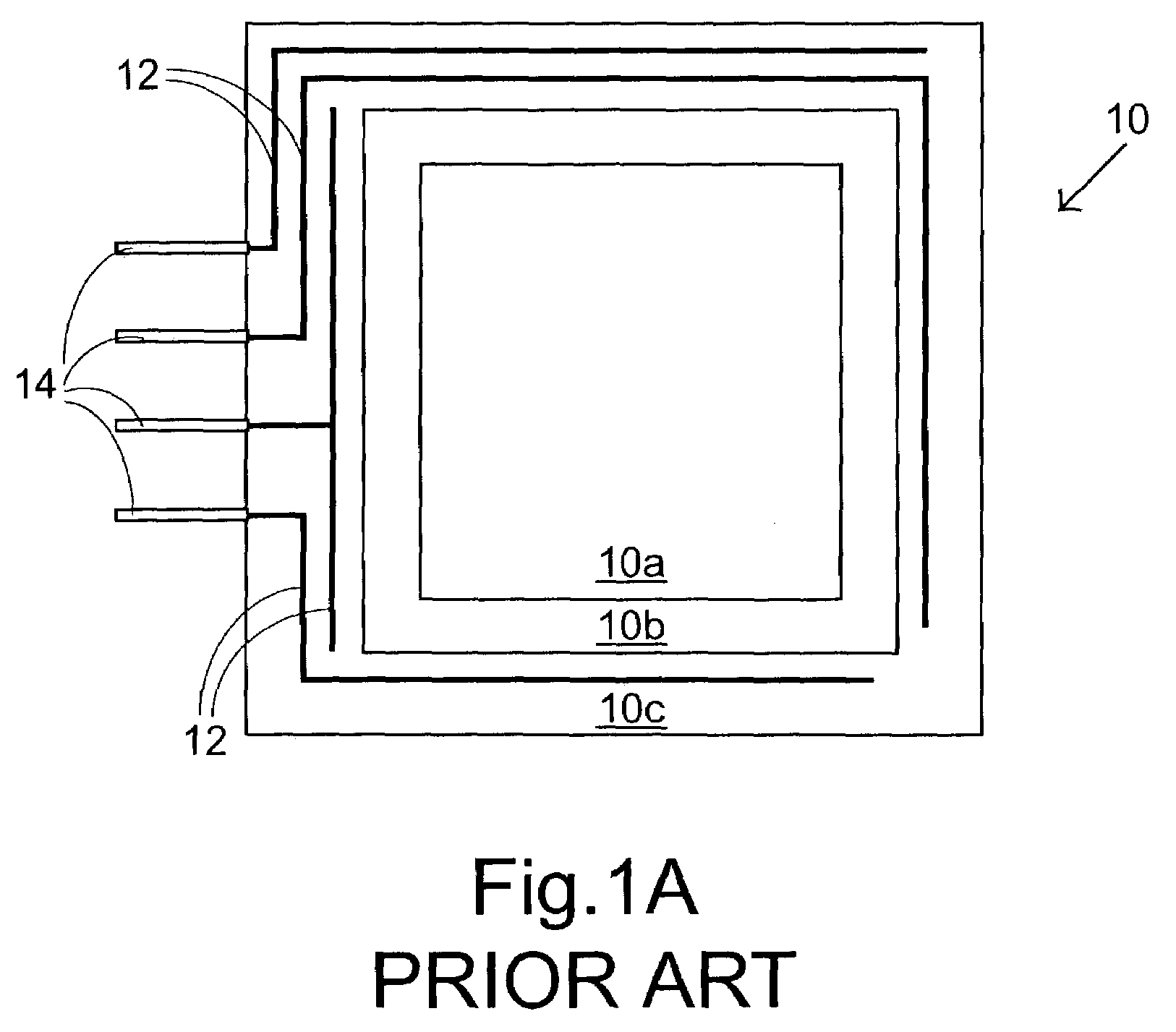
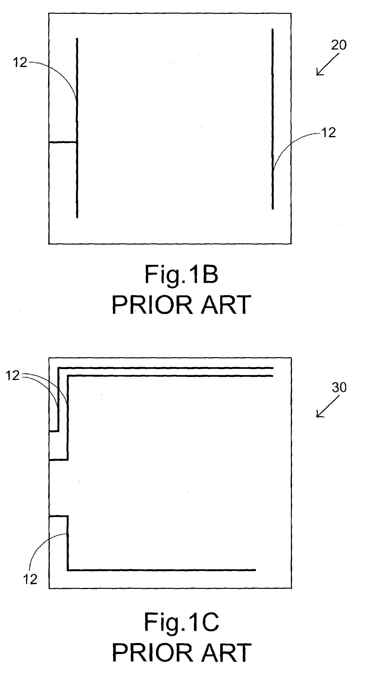
[0027]The present invention is related to a process for implementing conductive tracing layout in a touch panel, wherein the touch panel comprises two conductive substrates combined in parallel, and a gap between the conductive substrates. The gap is created by adhering spacer dots between the two conductive substrates. The conductive tracing is implemented on the opposite surfaces of two conductive substrates. According to the present invention, a conductive material is formed on the two conductive substrates by a deposition process such as Physical Vapor Deposition (PVD) or Chemical Vapor Deposition (CVD). Then, a precise conductive tracing layout can be produced on the two conductive substrates by way of the micro-lithographic technology. By the present process, the width of each of the conductive traces can be reduced to less than 0.1 mm. Besides, the signal loss during the signal transmission via the conductive traces can be minimized. The line-to-line space between every two c...


PUM

PropertyMeasurementUnit
widthaaaaaaaaaa
widthaaaaaaaaaa
widthaaaaaaaaaa

Abstract

The touch panel comprises two conductive substrates arranged in parallel and secured to each other with a gap existing between the conductive substrates The process for implementing a conductive tracing layout in a touch panel includes steps of forming a first conductive layer on at least one of the conductive substrates; forming a first photo-resist layer on the first conductive layer; removing a specified portion of the first photo-resist layer to form a first specified mask on a specified portion of the first conductive layer; and removing the first conductive layer except the specified portion of the first conductive layer to form a first conductive tracing layout.

Description

CROSS REFERENCE TO RELATED DOCUMENT[0001]This application claims priority to Taiwanese Patent Applications No. 091101770, filed on Feb. 01, 2002.FIELD OF THE INVENTION[0002]The present invention relates to a process for implementing a conductive tracing layout, and more particularly to a process for implementing a conductive tracing layout which is applied to a touch panel.BACKGROUND OF THE INVENTION[0003]A cathode ray tube (CRT) monitor has been gradually replaced by a liquid crystal display (LCD) due to the disadvantages of heavy weight, bulky size, and electromagnetic radiation. So far, an LCD has been extensively applied in various information products and communication products such as a notebook PC, mobile phone, portable PC, personal digital assistant (PDA), and so on. The interface of an information product or a communication product provided for a user to input data, for example, could be a touch panel or touch screen, which is attached on the screen of LCD. Then, the input...

Claims


Application Information

Patent Timeline
Patent Type & Authority Patents(United States)
IPC IPC(8): H01H11/00H01H11/02H01H11/04H01H65/00G06F3/033G06F3/041G06F3/048
CPCG06F3/0414G06F3/0488H01L2924/0002Y10T29/4916Y10T29/49105Y10T29/49117Y10T29/49124Y10T428/24917Y10T29/49227Y10T29/49155H01L2924/00
Inventor LIN, HONG-YUTSAI, YI-HUNG
Owner INNOLUX CORP
Why Eureka
Try Eureka