Semiconductor device and manufacturing method thereof

Active Publication Date: 2006-11-14
FUJITSU SEMICON LTD
View PDF26 Cites 3 Cited by
  • Summary
  • Abstract
  • Description
  • Claims
  • Application Information

AI Technical Summary

Benefits of technology

001] direction is made the moving direction of the carriers in the semiconductor element, thus r

Problems solved by technology

However, the roughness of the surface of the silicon substrate becomes high due to the aforementioned chemical solution treatment, and mobility of the carriers

Method used


Image

  • Semiconductor device and manufacturing method thereof
  • Semiconductor device and manufacturing method thereof
  • Semiconductor device and manufacturing method thereof

Examples


Example

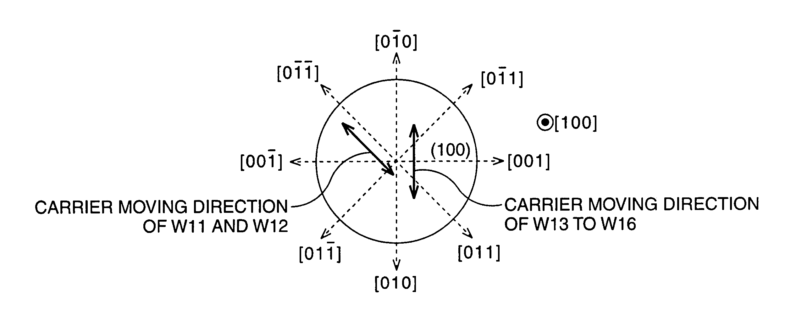
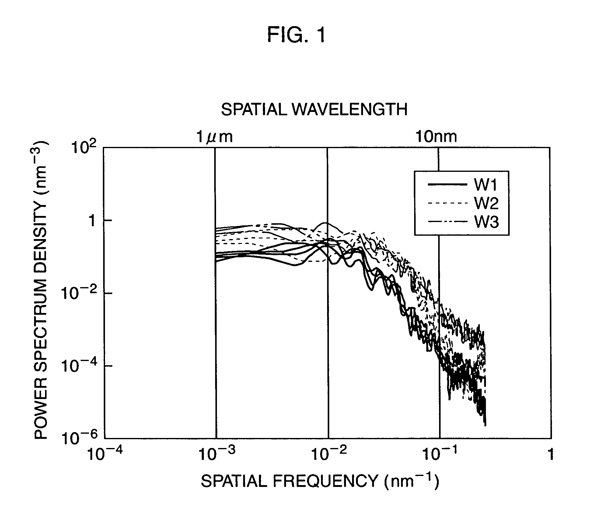
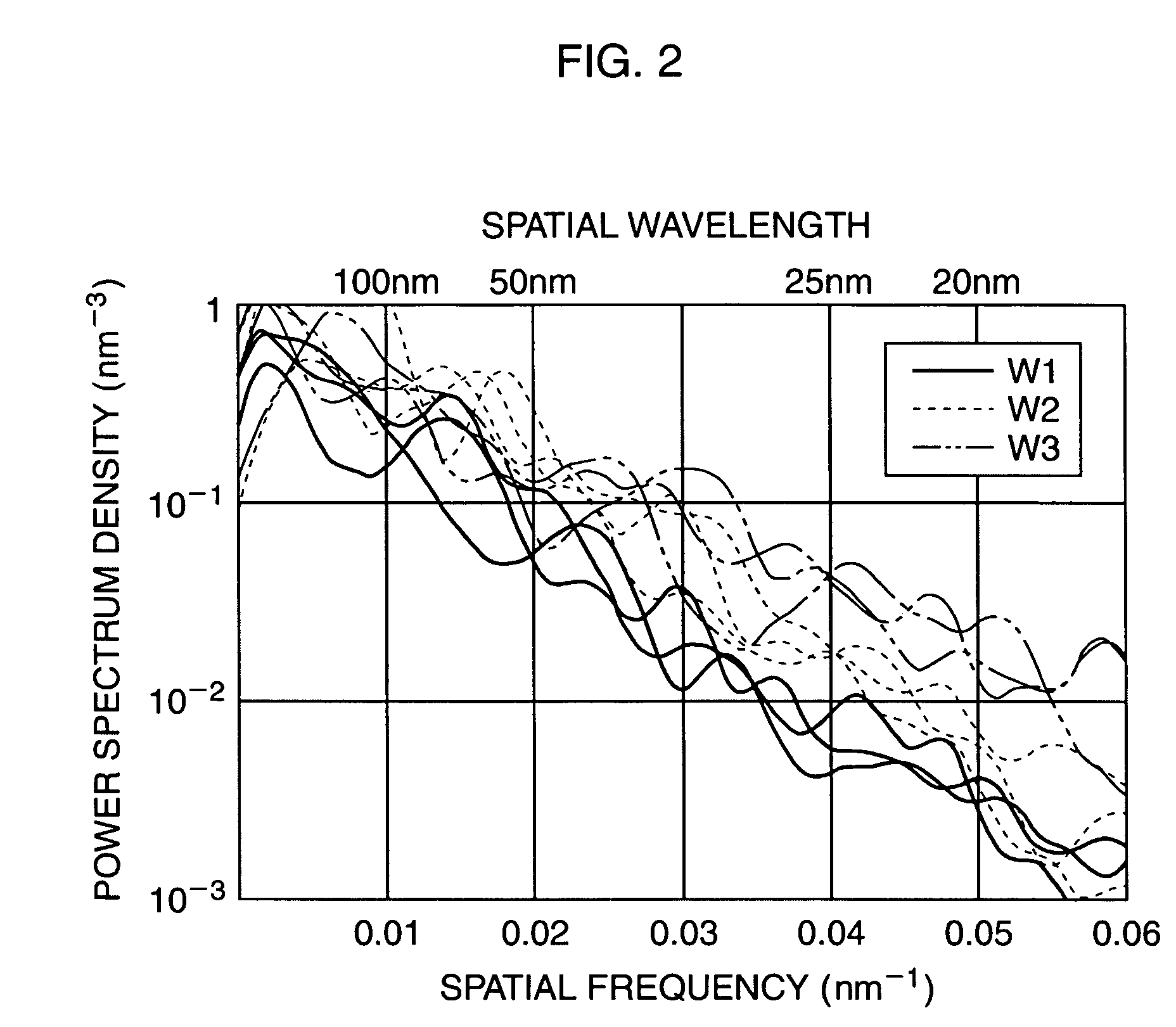
[0032]The inventor of the present application conducted the experiment concerning what influence the degree of the off-angle of a silicon substrate (semiconductor substrate) has on roughness of the surface of the silicon. In this experiment, after a bulk of single crystal silicon was produced by growing the single crystal silicon in the [100] direction by the CZ method, single crystal silicon substrates W1, W2 and W3 were cut while giving the off-angles as shown in the following Table 1 with respect to the (100) plane. After each of the single crystal silicon substrates was cleaned, thermal treatment was performed, whereby the steps existing on the surface were reconstituted. However, there is a possibility that an error exists in a range of ±0.03 degrees in the values in Table 1. The values in Table 1 are values obtained when the angle (off-angles) of the inclination of the normal of the surface of each of the silicon substrates was decomposed into the component in the [001] direct...


PUM


Abstract

Single crystal silicon is grown in a [100] direction to make a bulk. Next, a silicon substrate with a normal of a surface extending in an inclined direction from a [100] direction is cut from the bulk. At this time, when an angle (off-angle) of inclination of the normal is decomposed into a component in a [001] direction and a component in a [010] direction, the component in the [001] direction is made within ±0.2 degrees (excluding 0 degree). An MOS transistor with a moving direction of carriers being the [001] direction is formed on the surface of the silicon substrate. At this time, after steps existing on the surface of the silicon substrate are reconstituted by thermal treatment in a hydrogen atmosphere, a gate insulation film, a gate electrode and the like are formed.

Description

CROSS-REFERENCE TO RELATED APPLICATIONS[0001]This application is based upon and claims the benefit of priority from the prior Japanese Patent Application No. 2003-083064, filed on Mar. 25, 2003, the entire contents of which are incorporated herein by reference.BACKGROUND OF THE INVENTION[0002]1. Field of the Invention[0003]The present invention relates to a manufacturing method of a semiconductor device preferable for an MOS transistor and the like.[0004]2. Description of the Related Art[0005]In a manufacturing process of silicon substrates and a manufacturing process of semiconductor devices, chemical solution treatment for dissolving surface layers of silicon substrates is generally performed for the purpose of removing particles and removing metal contamination.[0006]Meanwhile, a surface of a silicon substrate is a plane which is intentionally inclined at about 0.2 to 0.5 degrees from a (100) plane. This is for preventing abnormal growth from occurring when an epitaxial layer is ...

Claims


Application Information

Patent Timeline
IPC IPC(8): H01L21/31H01L21/469H01L29/15H01L21/8234H01L21/28H01L21/324H01L21/8238H01L27/088H01L29/04H01L29/51H01L29/78
CPCH01L21/28185H01L21/28202H01L21/823807H01L29/045H01L29/513H01L29/518
Inventor KAWAMURA, HIROE
Owner FUJITSU SEMICON LTD
Why Eureka
Try Eureka