Semiconductor memory and its production process

Inactive Publication Date: 2006-11-14
FUJIO MASUOKA +1
View PDF20 Cites 31 Cited by
  • Summary
  • Abstract
  • Description
  • Claims
  • Application Information

AI Technical Summary

Benefits of technology

[0042]The present invention has been made in view of the above-mentioned problems. An object of the invention is to provide a semiconductor memory and a production process therefor, in which the degree of integration of the memory is improved by reducing the back

Problems solved by technology

That is, the larger the capacity between the floating gate and the control gate, the more effectively the potential of the control gate can be transmitted to the floating gate and the easier the writing and erasure become.
However, the thinning of the gate insulating film is limited in view of reliability of memory cells.
This is also questionable in view of reliability and is not practical.
This is, however, contradictory to the size reduction of memory cells and the capacity increase of EEPROM.
The selection gate lines can be formed continuously in self-alignment, but this is more difficult than the control gates 8 of the memory cells.
For, it is hard to form the diffusion layers selectively on the sidewalls of the pillar-form silicon layers.
For this reason, the number of memory cells connected in series is limited in view of the performance of memories.
Therefore, the

Method used


Image

  • Semiconductor memory and its production process
  • Semiconductor memory and its production process
  • Semiconductor memory and its production process

Examples


production example 1

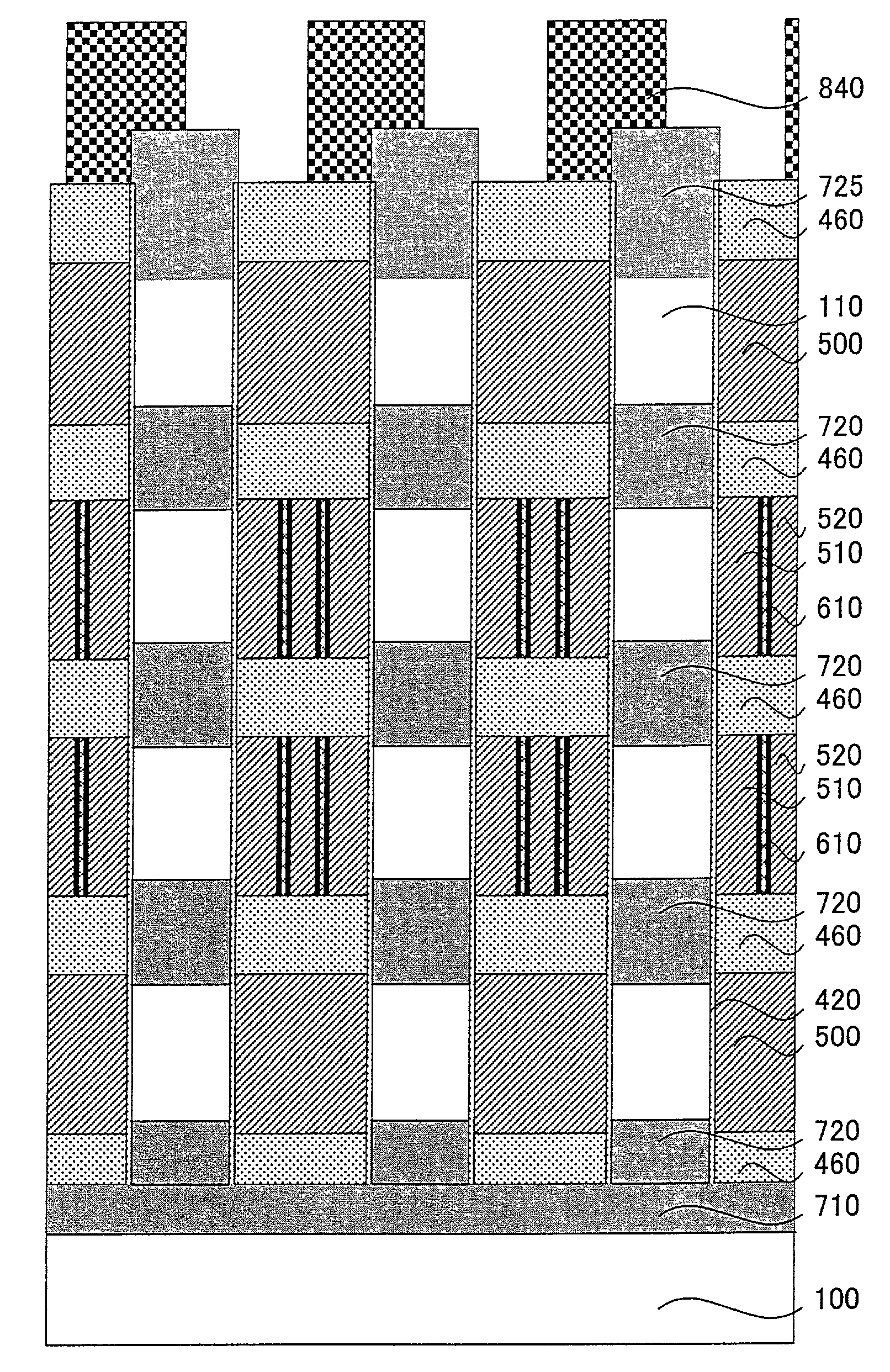
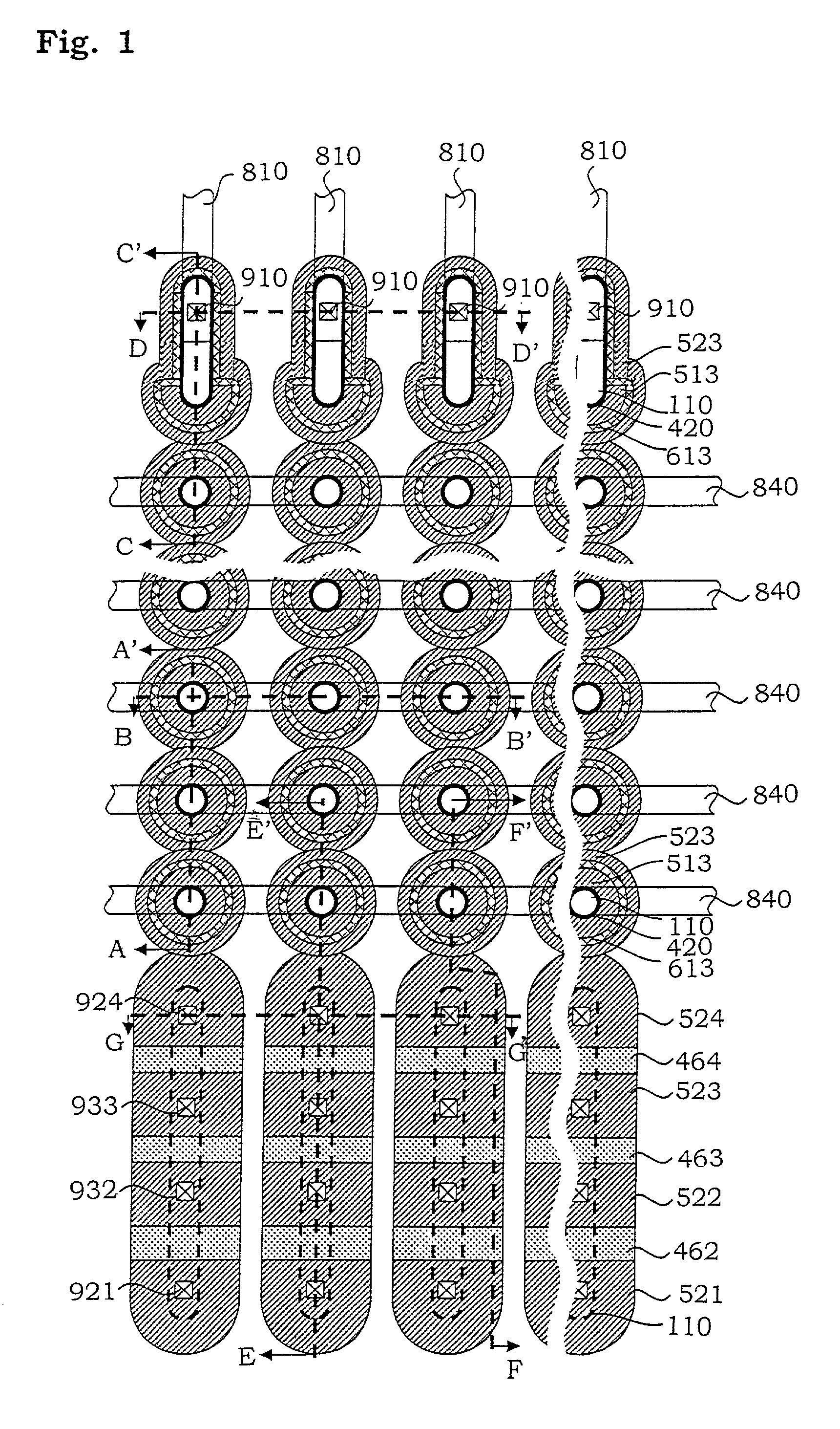
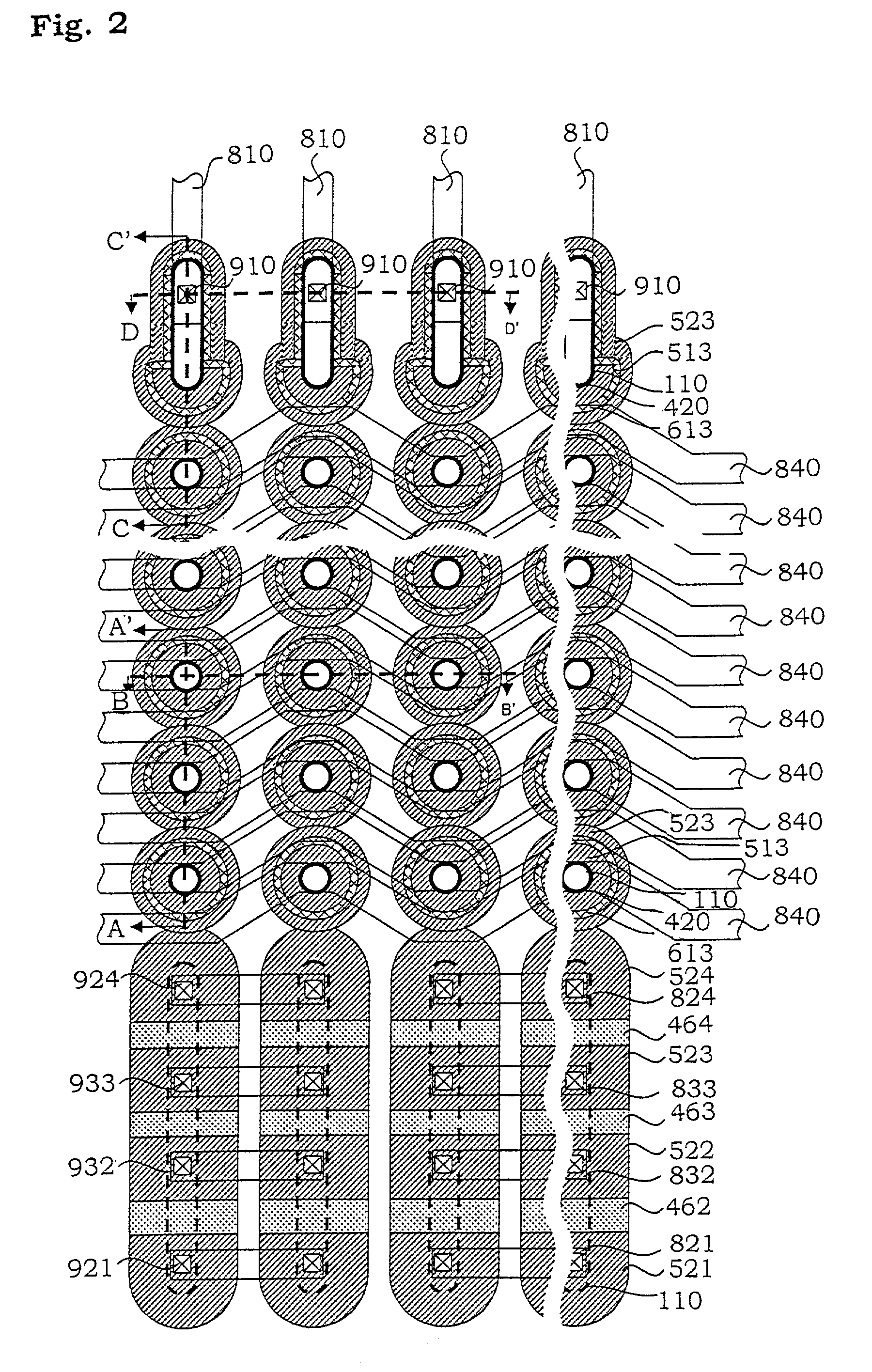
[0756]In a semiconductor memory to be produced in this example, a semiconductor substrate is patterned in the form of pillars to form island-like semiconductor layers. Sides of the island-like semiconductor layers make active regions. A plurality of tunnel oxide films and floating gates as charge storage layers are formed on the active regions. The island-like semiconductor layers are each in an electrically floating state with respect to the semiconductor substrate. The active region of each memory cell is in the electrically floating state. Selection gate transistors are disposed at the top and the bottom of the island-like semiconductor layer. A plurality of memory transistors, for example, two memory transistors, are placed between the selection gate transistors and are connected in series along the island-like semiconductor layer. The thickness of gate insulating films of the selection gate transistors is equal to the thickness of gate insulating films of the memory transistors...

production example 2

[0786]In the previous example, the memory cell has a floating gate structure for the charge storage layer. However, the charge storage layer is not necessarily of the floating gate structure. In this example, the charge storage is realized by the trapping of a charge into a laminated insulating film. The present invention is also effective in the case of an MNOS structure and an MONOS structure. The laminated insulating film here means a laminate structure of a tunnel oxide film and a silicon nitride film, or this laminate structure further with a silicon oxide film formed on the surface of the silicon nitride film. Next, explanation is given of an example of production of a memory cell of this structure.

[0787]In a semiconductor memory to be produced in this example, a semiconductor substrate is patterned in the form of pillars to form island-like semiconductor layers. Sides of the island-like semiconductor layers make active regions. A plurality of laminated insulating films as cha...

production example 3

[0808]In a semiconductor memory to be produced in this example, a semiconductor substrate is patterned in the form of pillars to form island-like semiconductor layers. Sides of the island-like semiconductor layers make active regions. A plurality of MIS capacitors as charge storage layers are formed on the active regions. The island-like semiconductor layers are each in an electrically floating state with respect to the semiconductor substrate. The active region of each memory cell is in the electrically floating state. One memory cell is constituted of one transistor and one capacitor. A plurality of memory cells, for example, two memory cells, are disposed on the island-like semiconductor layer and are connected in series along the island-like semiconductor layer. The thickness of gate insulating films of the transistors of the memory cells is equal to the thickness of capacitor insulating films of the capacitors of the memory cells. In this production example, the MIS capacitor a...


PUM


Abstract

A semiconductor memory comprises: a fist conductivity type semiconductor substrate and one or more memory cells constituted of an island-like semiconductor layer, a charge storage layer and a control gate, the charge storage layer and the control gate being formed to entirely or partially encircle a sidewall of the island-like semiconductor layer, wherein at least one of said one or more memory cells is electrically insulated from the semiconductor substrate.

Description

CROSS-REFERENCE TO RELATED APPLICATION[0001]This application is related to Japanese Patent Application No. 2000-286162 filed on 11, Aug. 2000, whose priority is claimed under 35 USC § 119, the disclosure of which is incorporated by reference in its entirety.BACKGROUND OF THE INVENTION[0002]1. Field of the Invention[0003]The present invention relates to a semiconductor memory and its production process, and more particularly, the invention relates to a semiconductor memory provided with a memory transistor having a charge storage layer and a control gate, and its production process.[0004]2. Description of Related Art[0005]As a memory cell of an EEPROM, is known a device of a MOS transistor structure having a charge storage layer and a control gate in a gate portion, in which an electric charge is injected into and released from the charge storage layer by use of a tunnel current. In this memory cell, data “0” and “1” is stored as changes in a threshold voltage by the state of the cha...

Claims


Application Information

Patent Timeline
IPC IPC(8): H01L27/108H01L29/94G11C16/04H01L21/28H01L21/336H01L21/8242H01L21/8244H01L21/8246H01L21/8247H01L21/84H01L27/11H01L27/115H01L27/12H01L29/788H01L29/792
CPCH01L21/28273H01L21/28282H01L21/84H01L27/11H01L27/1104H01L27/115H01L27/11556H01L27/11568H01L27/1203H01L29/66825H01L29/66833H01L29/7881H01L29/792G11C16/0483H01L27/10864H01L29/40114H01L29/40117H10B12/0383H10B10/00H10B10/12H10B69/00H10B41/27H10B43/30H01L29/788H10B99/00
Inventor ENDOH, TETSUOMASUOKA, FUJIOTANIGAMI, TAKUJIYOKOYAMA, TAKASHITAKEUCHI, NOBORU
Owner FUJIO MASUOKA
Why Eureka
Try Eureka