Semiconductor module and production method therefor and module for IC cards and the like

a technology applied in the field of semiconductor modules and production methods therefor, can solve the problems of poor flatness and smoothness, and the failure of the electric circuit of the ic chip to work, so as to improve the reliability, reduce the occurrence of defects, and improve the production yield

Inactive Publication Date: 2006-11-14
SHARP KK
View PDF29 Cites 28 Cited by
  • Summary
  • Abstract
  • Description
  • Claims
  • Application Information

AI Technical Summary

Benefits of technology

[0017]The present invention has been devised in view of what has been discussed above, it is therefore an object of the present invention to provide a semiconductor module which can prevent occurrence of defects accompanying penetration of moisture when exposed to a heavy environment such as a high temperature high humidity storage environment, a high temperature high humidity environment with a bias applied, a vapor pressurized environment or the like, which is comparable to the conditions of environment resistance tests on IC modules and which can reduce occurrence of defects in actual environment resistance tests and hence improve the production yield as well as improving the reliability under practical usage environments. That is, the object of the present invention is to provide such a semiconductor module and its production method and a module for IC cards and the like.

Problems solved by technology

However, when an attempt is made to make the print circuit board thinner, the handling performance after provision of the IC chip will deteriorate in the packaging process in module fabrication.
If an attempt was made to make there elements thinner, the IC chip would-break due to a bending load and would cause a fatal defect that causes the electric circuit of the IC chip not to work.
In reducing the thickness of the sealing resin, if the epoxy resin contains a lower amount of filler, the whole module becomes liable to warp due to stresses in the resin and hence presents poor flatness and smoothness for the electric terminal surface of a contact type IC card, causing contact failure with the electric connection terminal of the reader / writer device.
On the other hand, if the epoxy resin contains a large amount of filler, it presents poor fluidity and will produce unfilled portions.
When cooled from this condition, the moisture therein condenses and causes electric leakage in the interconnection circuit on the IC chip 4 surface and in printed wiring board 20, resulting in operation errors.

Method used


Image

  • Semiconductor module and production method therefor and module for IC cards and the like
  • Semiconductor module and production method therefor and module for IC cards and the like
  • Semiconductor module and production method therefor and module for IC cards and the like

Examples


Embodiment Construction

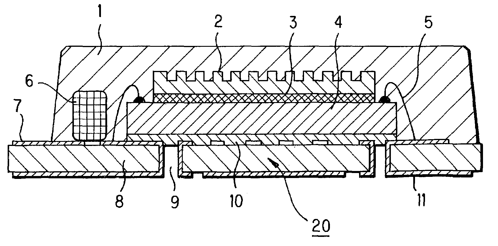
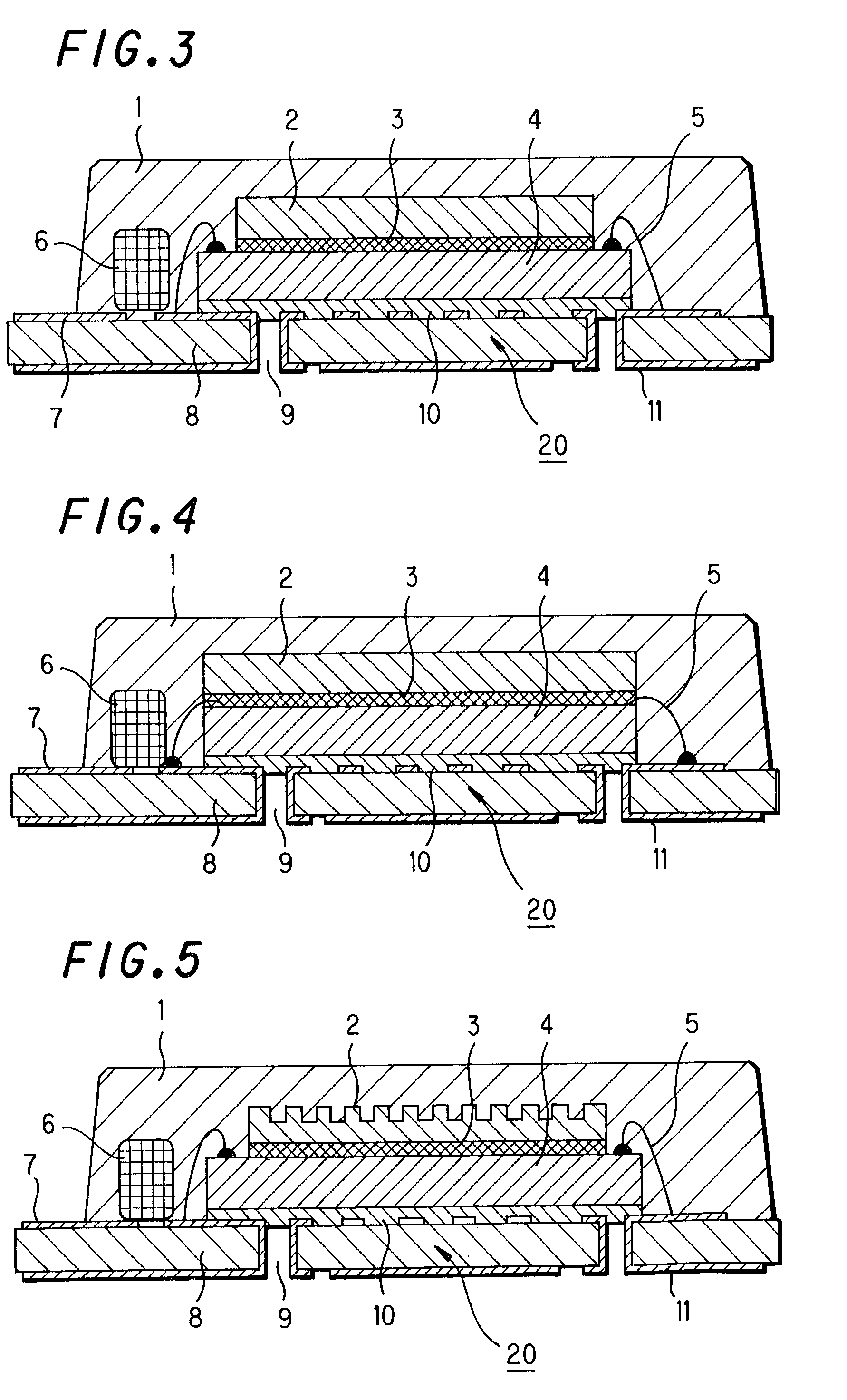
[0043]Referring next to FIG. 3 and other drawings, the preferred embodiments of semiconductor modules and their production method and a module for IC cards and the like according to the present invention will be described.

[0044]A double-sided printed wiring board 20 is comprised of an insulating layer 8 for polyimide double-sided interconnections, made up of glass epoxy impregnated with epoxy resin, having a thickness of 50 to 100 μm and a conductor which can be patterned by etching or other processes (forming aftermentioned antenna connection terminals 7 for the module and predetermined terminals 11 of printed wiring board 20) such as copper foil or the like, adhered on both sides of the insulator. This conductor is specified to have a thickness of 8 to 20 μm.

[0045]Here, in the present embodiment, a glass epoxy substrate having conductor layers of 12 μm thick on both sides thereof is shown as an example, but the conductor should not be limited particularly as long as it falls withi...


PUM


Abstract

A semiconductor module includes: a printed wiring board made of an insulator with conductor patterns formed on both sides thereof. An IC chip is mounted on the printed wiring board and sealed with a resin. A metallic sheet or moisture penetration blocking sheet is adhered on the IC chip surface opposite to the side that faces the printed wiring board.

Description

BACKGROUND OF THE INVENTION[0001](1) Field of the Invention[0002]The present invention relates to a module having an IC chip provided thereon and a packaging technique for its assembly. Detailedly, the present invention relates to a semiconductor module which can be reduced in thickness and can still provide high reliability of the peripheral parts against environmental conditions, as well as relating to the production method of the same and a module for IC cards and the like.[0003](2) Description of the Prior Art[0004]Recently, IC cards having a semiconductor integrated circuit device provided thereon have been put into practice as commutation tickets for public transportation such as buses, railroads and the like, financial cards including bank cards or identification cards. Since an IC card by itself has a data processing function and a high security function, which are not provided by magnetic cards, this advantage makes its application wider.[0005]The IC cards are categorized i...

Claims


Application Information

Patent Timeline
Patent Type & Authority Patents(United States)
IPC IPC(8): H01L23/28H01L23/04H01L23/48H01L23/52B42D15/10G06K19/077H01L21/56H01L21/60H01L23/00H01L23/12H01L23/29H01L23/31H01L23/433H01L23/498
CPCH01L23/49855H01L23/564H01L24/85H01L23/4334H01L2224/32225H01L2224/48091H01L2224/48225H01L2224/48227H01L2224/48465H01L2224/48471H01L2224/73265H01L2224/85148H01L2924/01004H01L2924/01006H01L2924/01013H01L2924/01014H01L2924/01029H01L2924/01033H01L2924/01078H01L2924/01079H01L2924/01082H01L2924/14H01L2924/16152H01L2924/19041H01L2924/19105H01L2924/00014H01L24/48H01L2924/01045H01L2924/014H01L2224/78H01L2224/45124H01L2224/45144H01L2924/00H01L2924/00012H01L24/45H01L2224/05554H01L2224/05624H01L2224/05647H01L2224/0566H01L2224/05686H01L2224/45015H01L2224/85399H01L2924/181H01L2924/20752H01L2924/20753H01L2924/05432H01L2924/013H01L2924/01404H01L23/12
Inventor NISHIKAWA, MASATAKA
Owner SHARP KK
Why Eureka
Try Eureka