Mount assembly, optical transmission line and photoelectric circuit board

a technology of optical transmission line and mounting assembly, applied in the direction of instruments, cladded optical fibres, optical elements, etc., can solve the problems of difficult to achieve the desired connection precision, increase the cost, and reduce the cost, so as to facilitate the connection of the mounting assembly and ease the requirement of perpendicularity. , the effect of reducing the transmission loss

Inactive Publication Date: 2006-11-14
PANASONIC CORP
View PDF10 Cites 4 Cited by
  • Summary
  • Abstract
  • Description
  • Claims
  • Application Information

AI Technical Summary

Benefits of technology

[0006]The inventors of the present invention have studied employing the spherical semiconductor device in an optical communication technology in view of the fact that optical communication tends to be employed in the field of electronic equipment. In the optical communication, a light signal may be required to be amplified in a communication line in some cases. For this purpose, another circuit (an amplifying circuit) may be provided in an optical communication system. This circuit derives a light signal from a fiber cable and converts the light signal to an electrical signal and then amplifies the electrical signal. The amplification circuit may result in lower speed and increased cost. Further, in the amplification circuit, it is generally difficult to achieve a desired connection precision upon connecting a light-receiving device and the optical fiber since a highly precise perpendicularity is required between the light signal which is emitted from the optical fiber and the light-receiving device.

Problems solved by technology

The amplification circuit may result in lower speed and increased cost.
Further, in the amplification circuit, it is generally difficult to achieve a desired connection precision upon connecting a light-receiving device and the optical fiber since a highly precise perpendicularity is required between the light signal which is emitted from the optical fiber and the light-receiving device.
Although the technology disclosed in the above-mentioned documents makes it possible to obtain an excellent effect employing a feature conferred by the spherical shape of the semiconductor, a sufficiently practical mount structure has not been achieved and therefore the application thereof is limited.
Further, the geometrical feature of the spherical semiconductor device is not sufficiently recognized and it is predominantly considered that a planar super-svelte chip semiconductor is enough to be mounted on a product.

Method used


Image

  • Mount assembly, optical transmission line and photoelectric circuit board
  • Mount assembly, optical transmission line and photoelectric circuit board
  • Mount assembly, optical transmission line and photoelectric circuit board

Examples


first embodiment

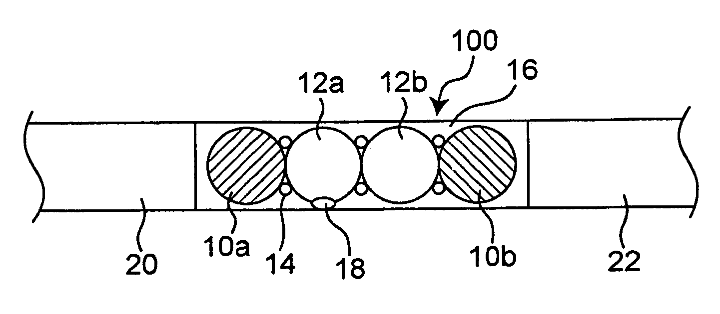
[0053]FIG. 1 is a side view showing a first embodiment of the present invention. This embodiment is an example of a mount assembly which has a function of amplifying a light signal. This mount assembly may be used as, for example, an optical relay module for high-speed and high-capacity data communication.

[0054]This mount assembly 100 is disposed between two optical fibers 20 and 22 which are optical transmission lines. This mount assembly 100 amplifies a light signal that is emitted from the optical fiber 20 and then makes the light signal enter into the optical fiber 22. The mount assembly 100 has two spherical photoelectric conversion devices, and one of them is a photo-electro conversion device 10a and the other is an electro-photo conversion device 10b. The mount assembly 100 also has two spherical semiconductor devices 12a and 12b as an amplifier, which are disposed between the photoelectric semiconductor devices 10a and 10b. These four devices are arranged in a line and the a...

second embodiment

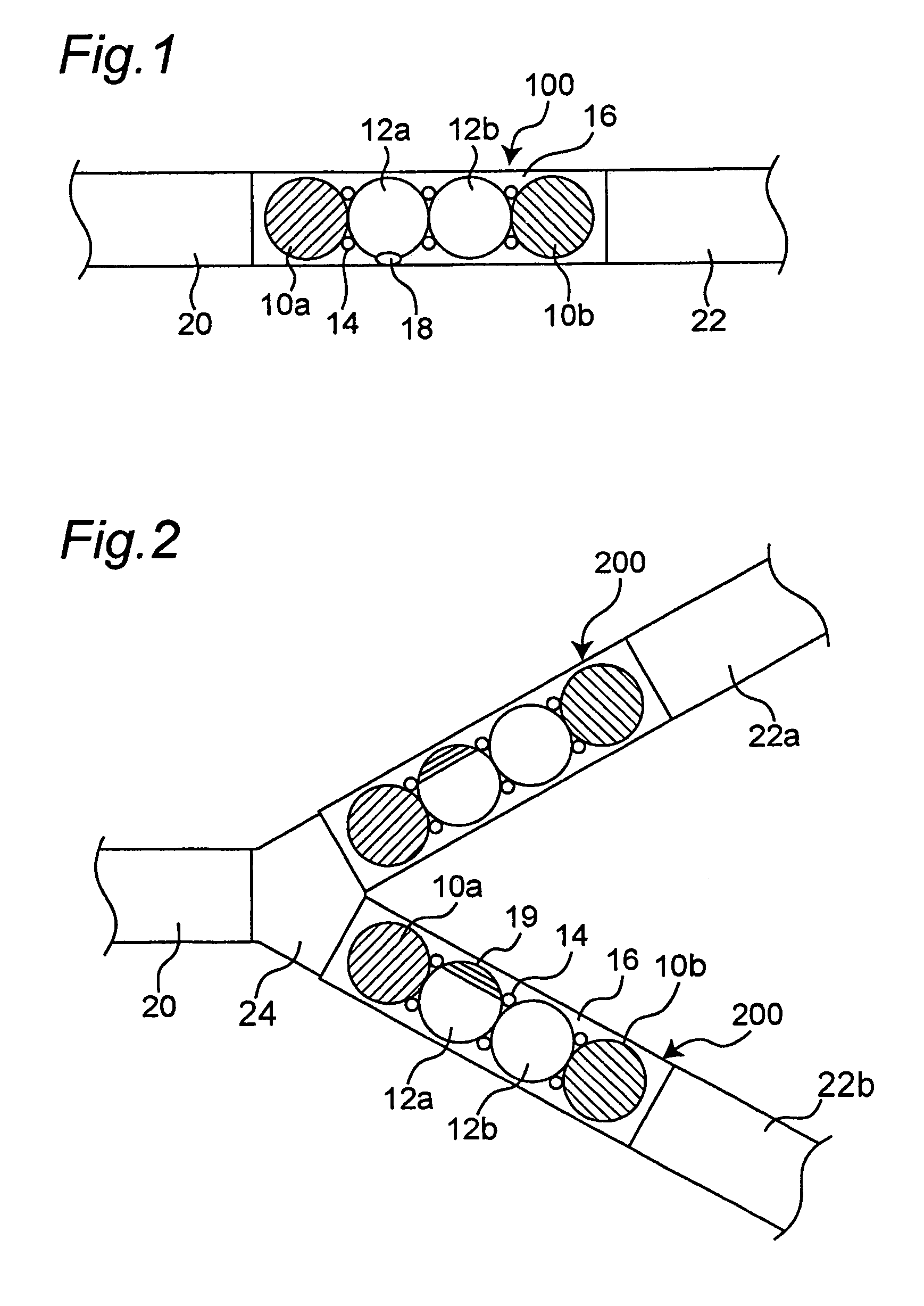
[0072]FIG. 2 schematically shows a plan view of a second embodiment of the present invention. FIG. 2 shows an embodiment wherein mount assemblies 200 of the present invention are disposed in a branch portion of an optical fiber. When a signal is transmitted through the optical fiber, it is often necessary to divide the signal. The signal intensity may be reduced when dividing the signal optically, which is disadvantageous to the signal transmission. In order to avoid or reduce such disadvantage, the mount assembly of the present invention can be used. In the illustrated embodiment, a light signal transmitted through an optical fiber 20 is divided at a branch joint 24 and transmitted to right-hand optical fibers 22a and 22b respectively as viewed in FIG. 2. Each of the mount assemblies 200 of the present invention is provided as an optical relay module and disposed between the branch joint 24 and each of the optical fibers 22a and 22b to amplify the divided light signal and transmit ...

third embodiment

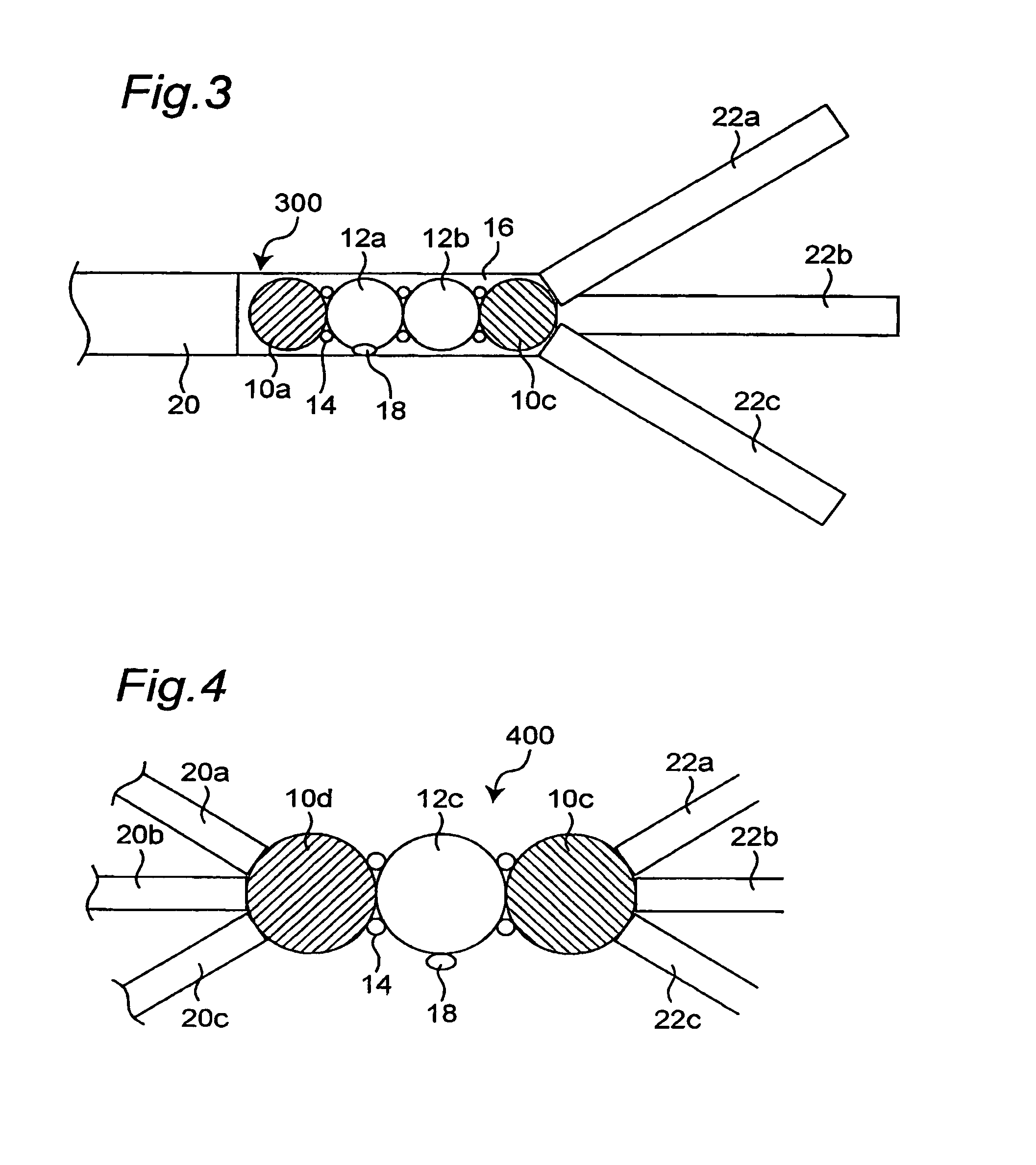
[0074]FIG. 3 schematically shows a plan view of a third embodiment of the present invention. FIG. 3 shows another embodiment wherein an optical fiber is branched using a mount assembly 300 of the present invention.

[0075]In this embodiment, a light signal from an optical fiber 20 is divided and transmitted in a plurality (three in FIG. 3) of right-hand optical fibers 22a, 22b and 22c as viewed in FIG. 3. In the mount assembly 300 of the present invention, a electro-photo conversion device 10c is constructed so as to emit light in three directions. Also in the mount assembly 300, since the electro-photo conversion device 10c is spherical, light signals can be derived from a plurality of positions and coupled to a plurality of optical fibers when optical devices are disposed at three positions as shown in FIG. 13C or an entire semispherical surface close to the optical fibers 22a, 22b and 22c is made to be a light-emitting portion. A resin 16, which covers the mount assembly 300, is ma...


PUM


Abstract

A mount assembly which amplifies a light signal from an optical transmission line and transmits the light signal to another optical transmission line and does not require a highly precise perpendicularity at a connection portion between the optical transmission line and the mount assembly. The mount assembly (100) is obtained by connecting a photo-electro conversion device (10a), spherical semiconductor devices (12a) and (12b) and an electro-photo conversion device (10b) through electrical-connection portions (14) so that a light received by the photo-electro conversion device (10a) is amplified by the spherical semiconductor devices (12a) and (12b) and then emitted from the electro-photo conversion device (10b).

Description

CROSS-REFERENCE TO RELATED APPLICATIONS[0001]The present application claims priority under 35 U.S.C. §119 to Japanese Patent Application No. 2003-189339 filed on Jul. 1, 2003, entitled “Spherical semiconductor device and mount assembly using the same and electronic equipment using the same.” The contents of that application are incorporated herein by reference thereto in their entirety.TECHNICAL FIELD[0002]The present invention relates to a mount assembly wherein a spherical photoelectric conversion device and a spherical semiconductor device that forms an electronic circuit are electrically connected to each other, and an optical transmission line and a photoelectric circuit board which use the mount assembly.BACKGROUND OF THE INVENTION[0003]In the field of electronic equipment, such as a cellular phone, a book-size personal computer and a PDA (personal digital assistance) which all require high-speed communication, a production which realizes higher-speed communication is desired ...

Claims


Application Information

Patent Timeline
Patent Type & Authority Patents(United States)
IPC IPC(8): G02B6/12H01L31/00G02B6/02G02B6/43H01L23/52H01L27/00H01L31/0352H01L33/20H01L33/24
CPCG02B6/43H01L31/035281H01L33/20H01L33/24Y02E10/50H01L2924/1017H01L2224/16225G02B6/02G02B6/12H01L23/52H01L27/00
Inventor NISHIYAMA, TOUSAKUISHIMARU, YUKIHIROSUGAYA, YASUHIROASAHI, TOSHIYUKIKARASHIMA, SEIJI
Owner PANASONIC CORP
Why Eureka
Try Eureka