DRAM constructions, memory arrays and semiconductor constructions

a technology of memory arrays and semiconductors, applied in the direction of transistors, solid-state devices, capacitors, etc., can solve the problems of difficult to pattern platinum into a desired shape, smear platinum, and use noble metals in metal patterning constructions

Inactive Publication Date: 2006-11-28
MICRON TECH INC
View PDF7 Cites 6 Cited by
  • Summary
  • Abstract
  • Description
  • Claims
  • Application Information

AI Technical Summary

Problems solved by technology

A difficulty in utilizing the noble metals is in patterning constructions from the metals.
For instance, if platinum is utilized to form a conductive component of a capacitor construction, it can be difficult to pattern the platinum into a desired shape.
However, such method can smear platinum.
The smearing can cause undesirable defect structures.

Method used


Image

  • DRAM constructions, memory arrays and semiconductor constructions
  • DRAM constructions, memory arrays and semiconductor constructions
  • DRAM constructions, memory arrays and semiconductor constructions

Examples


Embodiment Construction

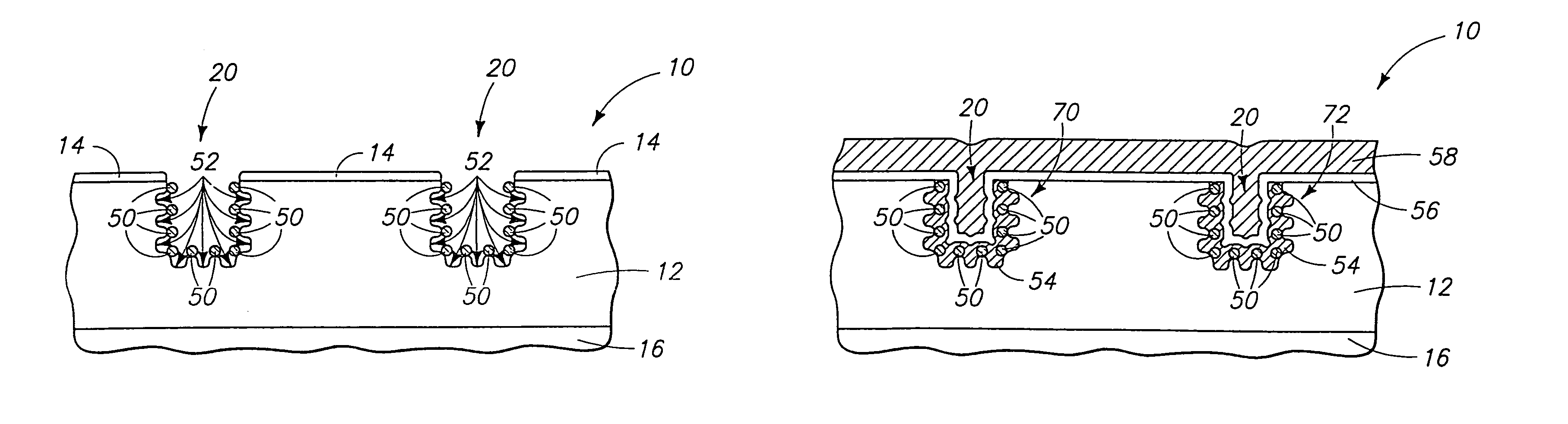
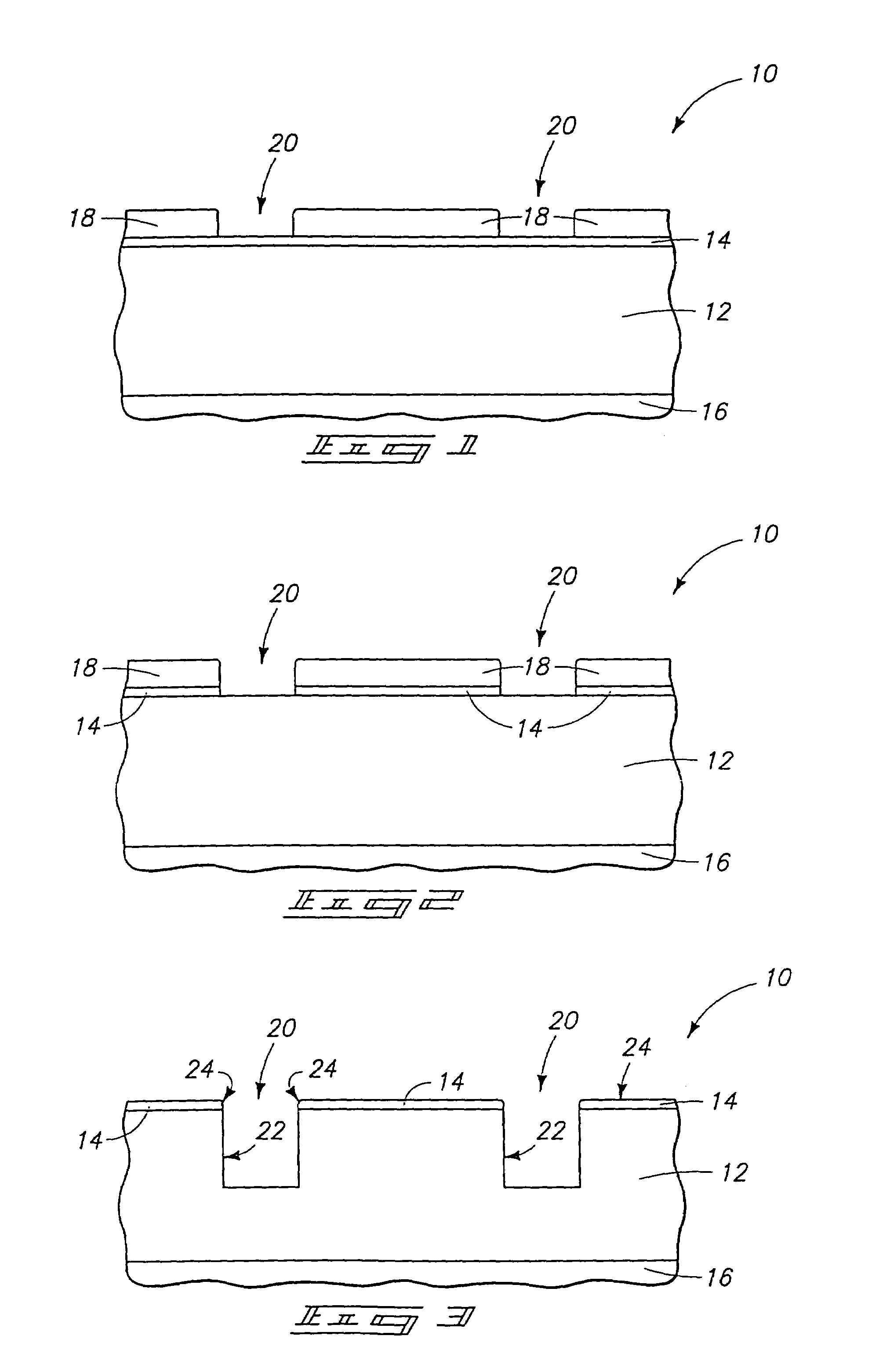
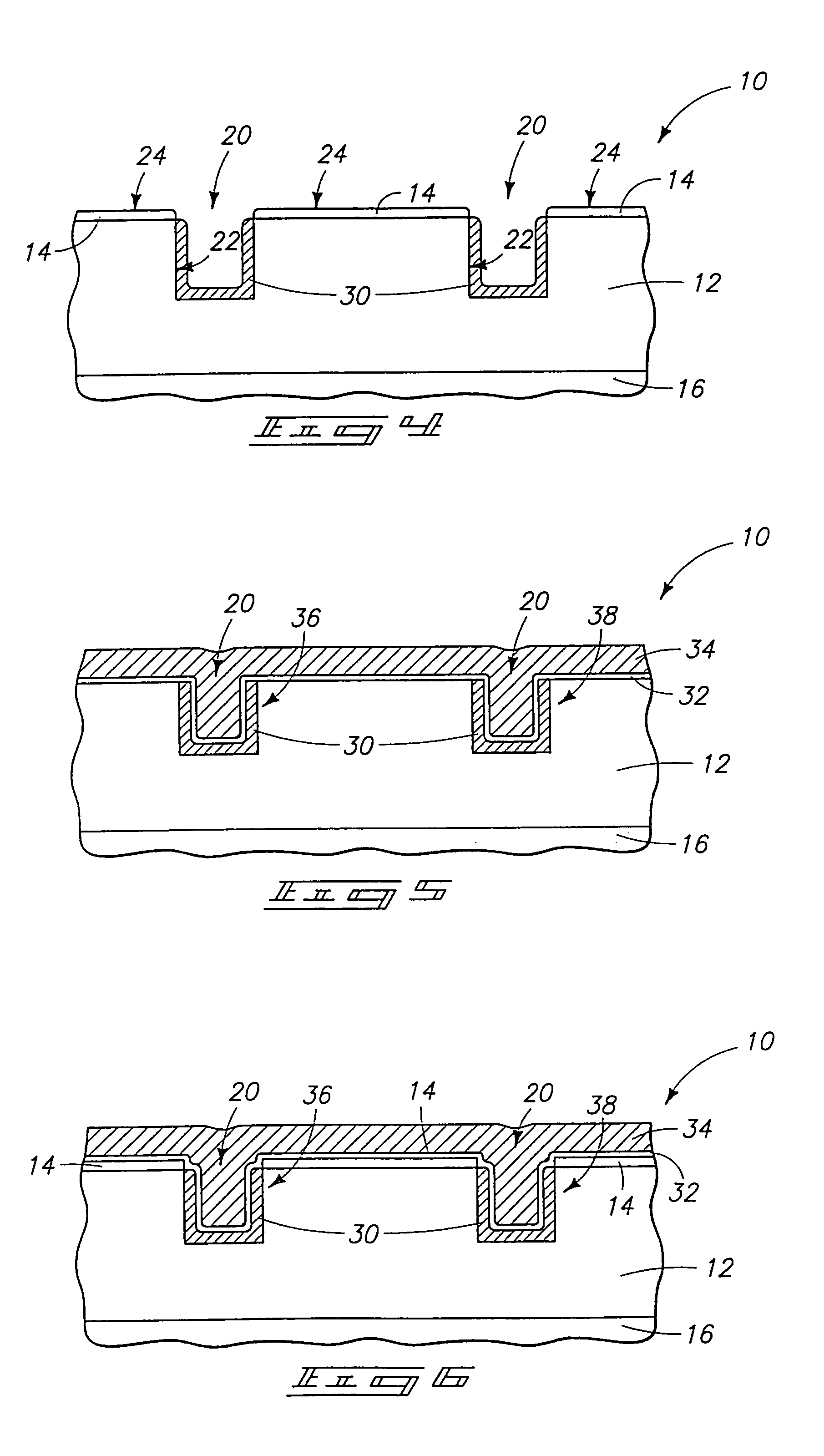
[0023]One aspect of the invention is a recognition that deposition of platinum and other noble metals can be substrate dependent under appropriate processing conditions. Specifically, it is found that noble metals can be preferentially deposited on either borophosphosilicate glass (BPSG) or tantalum oxide substrates relative to non-oxidized doped silicon (such as, for example, doped polycrystalline silicon). Further, it is found that appropriate processing conditions will selectively deposit noble metals on BPSG or tantalum oxide (such as, for example, tantalum pentoxide) relative to aluminum oxide (Al2O3). Additionally, it is found that appropriate processing can provide a rate of deposition which is selective for various different kinds of oxides and doped non-oxidized silicon in the order that the deposition is selective for BPSG relative to thermally-formed silicon dioxide, and selective for both BPSG and thermally-formed silicon dioxide relative to doped non-oxidized silicon.

[0...


PUM


Abstract

The invention includes a method of depositing a noble metal. A substrate is provided. The substrate has a first region and a second region. The first and second regions are exposed to a mixture comprising a precursor of a noble metal and an oxidant. During the exposure, a layer containing the noble metal is selectively deposited onto the first region relative to the second region. In particular applications, the first region can comprise borophosphosilicate glass, and the second region can comprise either aluminum oxide or doped non-oxidized silicon. The invention also includes capacitor constructions and methods of forming capacitor constructions.

Description

RELATED PATENT DATA[0001]This patent resulted from a continuation application of U.S. patent application Ser. No. 10 / 773,780 which was filed Feb. 9, 2004, and is now U.S. Pat. No. 6,858,894; which in turn resulted from a divisional application of U.S. patent application Ser. No. 10 / 231,789, which was filed Aug. 29, 2002, and is now U.S. Pat. No. 6,773,984.TECHNICAL FIELD[0002]The invention pertains to methods of depositing noble metals. The invention also pertains to methods of forming capacitor constructions, as well as to the capacitor constructions themselves.BACKGROUND OF THE INVENTION[0003]Capacitors are utilized in numerous semiconductor constructions, including, for example, dynamic random access memory (DRAM) devices. Capacitors comprise a pair of electrically conductive materials (frequently referred to as a storage node and a capacitor plate) which are separated from one another by dielectric material. The conductive materials are thus capacitively coupled with one another...

Claims


Application Information

Patent Timeline
Patent Type & Authority Patents(United States)
IPC IPC(8): H01L29/94H01L21/8242H01L21/02H01L21/334H01L21/4763H01L27/108H01L29/76H01L31/119
CPCH01L27/1087H01L28/65H01L28/84H01L27/1085H01L27/10852H01L29/66181H10B12/0387H10B12/033H10B12/03
Inventor SRIVIDYA, CANCHEEPURAM V.GEALY, F. DANIELGRAETTINGER, THOMAS M.
Owner MICRON TECH INC
Why Eureka
Try Eureka