Memory interface system and method for reducing cycle time of sequential read and write accesses using separate address and data buses

a memory interface and data bus technology, applied in the field of memory interface systems and methods, can solve the problems that the memory access cannot be quickly followed by the other memory access, and achieve the effects of reducing cycle time, increasing throughput, and substantially increasing data throughput across the data bus

Active Publication Date: 2006-11-28
INFINEON TECH LLC
View PDF3 Cites 53 Cited by
  • Summary
  • Abstract
  • Description
  • Claims
  • Application Information

AI Technical Summary

Benefits of technology

[0015]The problems outlined above are solved by an improved semiconductor memory and, more specifically, a QDR SRAM that can output data in multiples of each every clock cycle of the system clock. The system clock, synchronous with the data strobe, is sent with the control bus between the functional elements of the CPU, memory, and I/O interface. By transferring data to and from the memory each one-half clock cycle of the system clock, data throughput across the data bus is substantially increased. To take full advantage of this increased throughput, however, cycle times of a read operation, followed by a write operation (i.e., read access followed by a write

Problems solved by technology

Even with fast access time associated with SRAM, one memory

Method used


Image

  • Memory interface system and method for reducing cycle time of sequential read and write accesses using separate address and data buses
  • Memory interface system and method for reducing cycle time of sequential read and write accesses using separate address and data buses
  • Memory interface system and method for reducing cycle time of sequential read and write accesses using separate address and data buses

Examples


Embodiment Construction

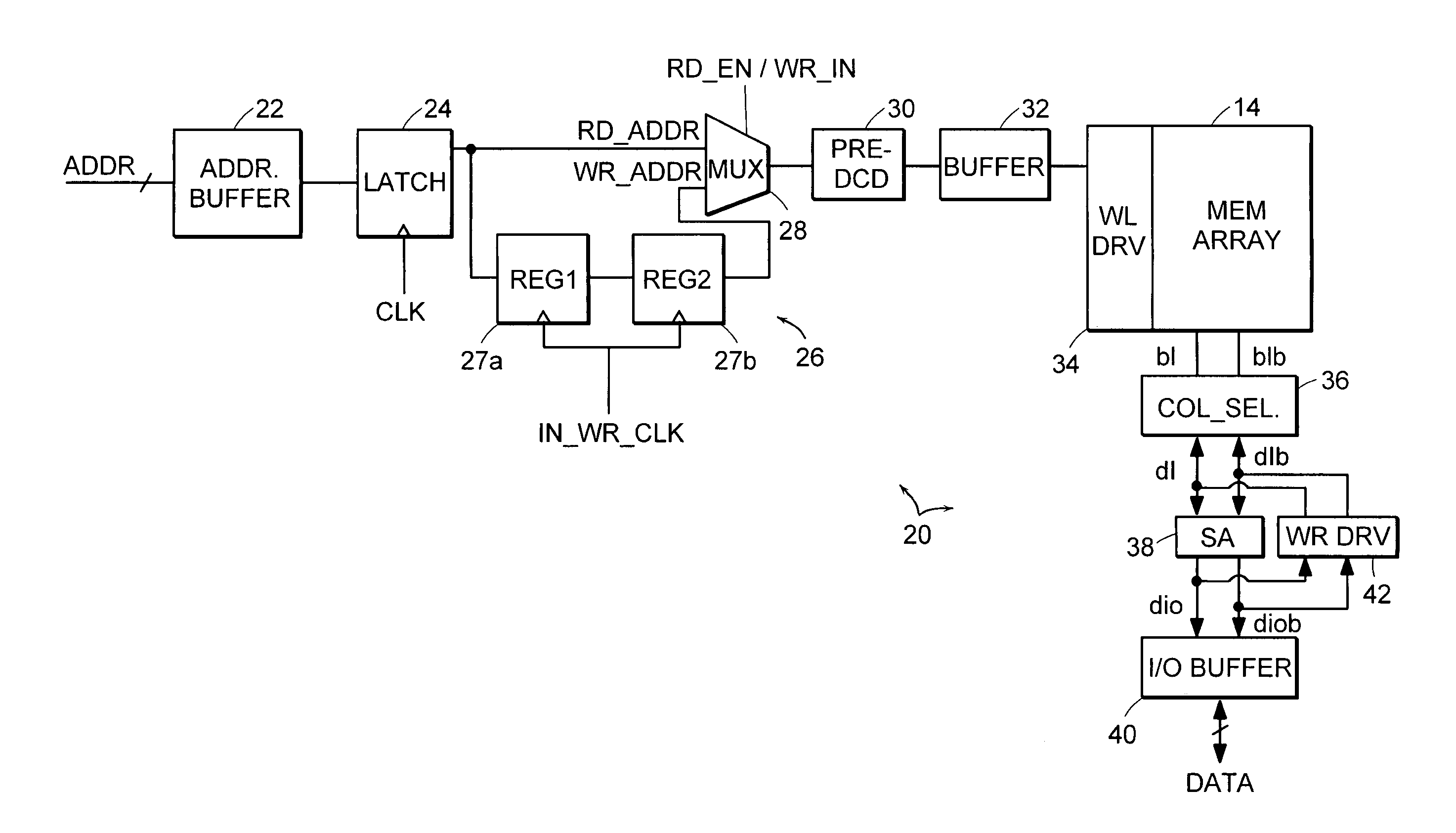
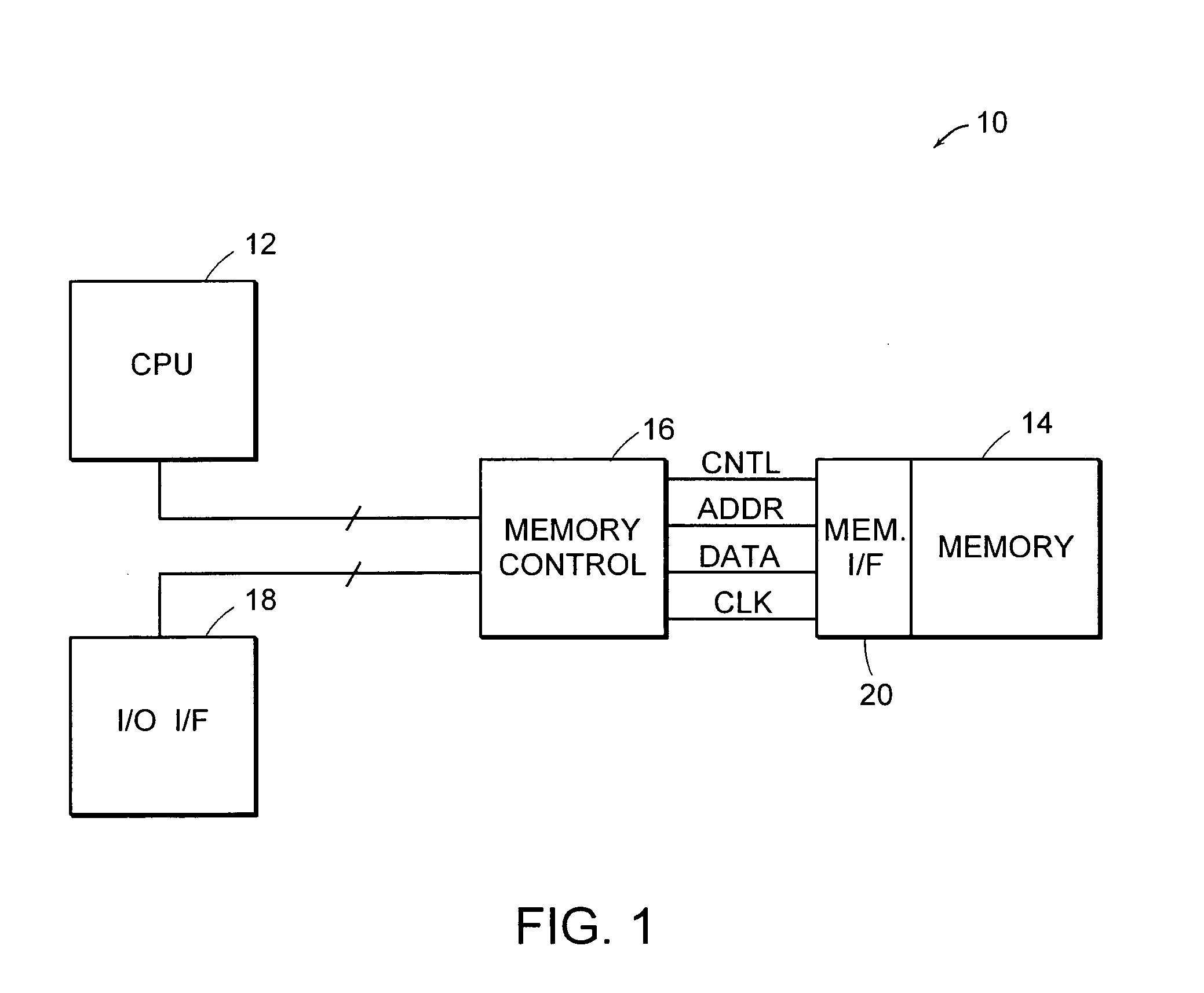
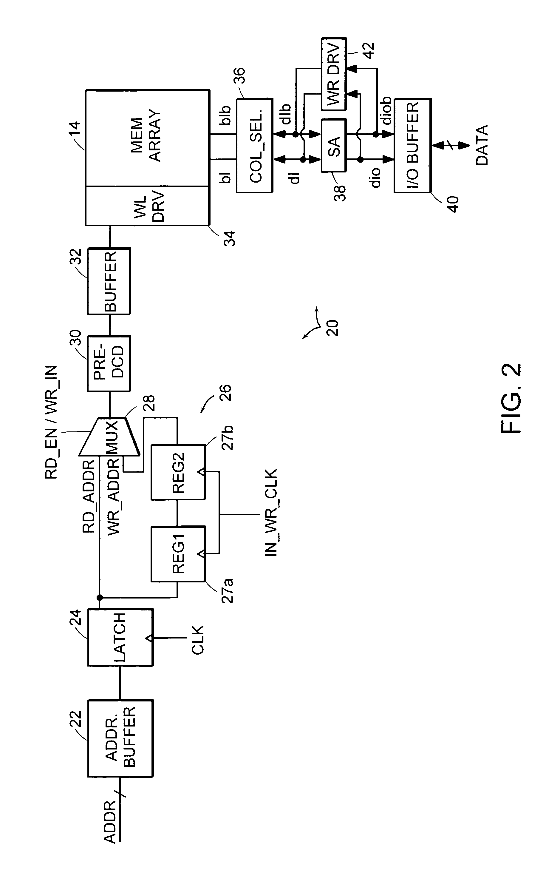
[0029]Turning now to the drawings, FIG. 1 illustrates various functional blocks of a computing system 10. System 10 includes a microprocessor or CPU 12. CPU 12 is oftentimes referred to as an execution engine or processor. Most CPUs are known to incorporate two operational units: an integer unit and a floating-point unit. These units communicate data via a data cache and are controlled by a single instruction stream supplied by an instruction cache. The data cache and instruction cache can be connected to memory 14 if desired by a memory controller 16. The instruction cache can supply multiple instructions per fetch if, for example, CPU 12 is a superscalar processor. The actual number of instructions fetched can vary. As the instructions are dispatched from the instruction cache, a decoder will decode those instructions and place them into a prefetch unit, and finally into the execution engine. Any out-of-order conditions can be resolved by a reorder buffer, which places those instr...


PUM


Abstract

A memory interface system and method are provided for transferring data between a memory controller and an array of storage elements. The storage elements are preferably SRAM elements, and the memory interface is preferably one having separate address bus paths and separate data bus paths. One address bus path is reserved for receiving read addresses and the other address bus path is reserved for receiving write addresses. One of the data bus paths is reserved for receiving read data from the array, and the other data bus path is reserved for receiving data written to the array. While bifurcating the address and data bus paths within the interface is transparent to the memory controller, the separate paths afford addressing phases of a read and write address operation to be partially overlapped, as well as the data transfer phases. This will essentially reduce the cycle time between a read and write memory access, and proves useful when maximizing the data throughput across the data bus when implementing double data rate (QDR) mechanisms.

Description

BACKGROUND OF THE INVENTION[0001]1. Field of the Invention[0002]This invention relates to semiconductor memory and, more particularly, to a memory interface that transparently separates the read and write address and data buses to achieve a faster sequential read and write cycle time.[0003]2. Description of the Related Art[0004]The following descriptions and examples are not admitted to be prior art or conventional by virtue of their inclusion within this section.[0005]Most computing systems consist of four functional blocks: a microprocessor (or CPU), memory, input / output (I / O) interface, and an I / O device. The CPU is interconnected to the memory and the I / O interface via an address bus and a data bus. The address bus provides a path in which the CPU can select certain storage locations in which data is stored. The data bus provides a path over which data is transferred between the CPU, memory, and the I / O interface. Most microprocessors handle bits in 16, 32, or 64 bit groups. Thu...

Claims


Application Information

Patent Timeline
IPC IPC(8): G11C8/00
CPCG11C7/1066G11C8/18G11C11/417
Inventor TRAN, THINHTZOU, JOSEPHPARAMESWARAN, SURESH
Owner INFINEON TECH LLC
Why Eureka
Try Eureka