Semiconductor memory card access apparatus, a computer-readable recording medium, an initialization method, and a semiconductor memory card

a technology of semiconductor memory card and access apparatus, which is applied in the direction of memory adressing/allocation/relocation, instruments, and unauthorized memory use protection, can solve the problem of significantly shortening the time required for writing data, and achieve the effect of accurately accessing the user area

Inactive Publication Date: 2006-11-28
PANASONIC CORP
View PDF15 Cites 22 Cited by
  • Summary
  • Abstract
  • Description
  • Claims
  • Application Information

AI Technical Summary

Benefits of technology

[0011]An object of the present invention is to provide an access apparatus that achieves a reduction in the processing time required to modify erasable blocks, as well as forming a data storage format in a semiconductor memory card that enables a nonvolatile memory having a longer lifespan to be realized.
[0013]In order to achieve the above-mentioned object, the semiconductor memory card access apparatus may have the following structure. The access apparatus performs file access on a semiconductor memory card that has a memory area comprising a plurality of sectors by managing data in each group of 2j sectors (j being 0 or a positive integer) as a cluster, and managing one or more clusters as a file. Here, each group of 2i consecutive sectors in the memory area forms a block (i being 0 or a positive integer), which is the smallest unit on which data erasure can be performed. The access apparatus includes a calculation unit, a reserving unit, and a recording unit. The calculation unit calculates a size of volume management information based on a number of clusters in the memory area that are to be managed. Here, the volume management information includes a file allocation table that indicates, for each file, links between clusters corresponding to the file. The reserving unit reserves a first area for recording the volume management information, and a second area for recording user data. The first area has a data size larger than the calculated volume management information, and is formed from m×2j sectors (m being a positive integer), while the second area is formed from sectors following the first area. The recording unit records volume management information in the first area, and user data in the second area, and manages the volume management information and the user data as clusters. In this access apparatus, an area in the volume area having m clusters (m is a positive integer) is reserved for recording volume management information, so there is no possibility of any cluster being stored straddling two erasable blocks. Cluster boundaries can be aligned with erasable block boundaries, and the boundary of the volume management information can be aligned with an erasable block boundary. Consequently, only one erasable block needs to be erased when a cluster is rewritten or overwritten, and the number of times that erasable blocks have to be erased can be reduced. If the number of block erasures is reduced, the semiconductor memory card can write data in a shorter time, and the lifespan of the nonvolatile memory itself can be increased.
[0016]Here, the recording unit may set the predetermined number of sectors in the partition table recording the volume management information. In this structure, even if the size of the first area changes, causing the start address of the second area to change, a number of sectors, obtained by subtracting 1 from the number of sectors NOM, is set in the partition table, so the access apparatus can access the user area accurately by referring to the partition table.

Problems solved by technology

As a result, the time required to write data is significantly lengthened.

Method used


Image

  • Semiconductor memory card access apparatus, a computer-readable recording medium, an initialization method, and a semiconductor memory card
  • Semiconductor memory card access apparatus, a computer-readable recording medium, an initialization method, and a semiconductor memory card
  • Semiconductor memory card access apparatus, a computer-readable recording medium, an initialization method, and a semiconductor memory card

Examples


second embodiment

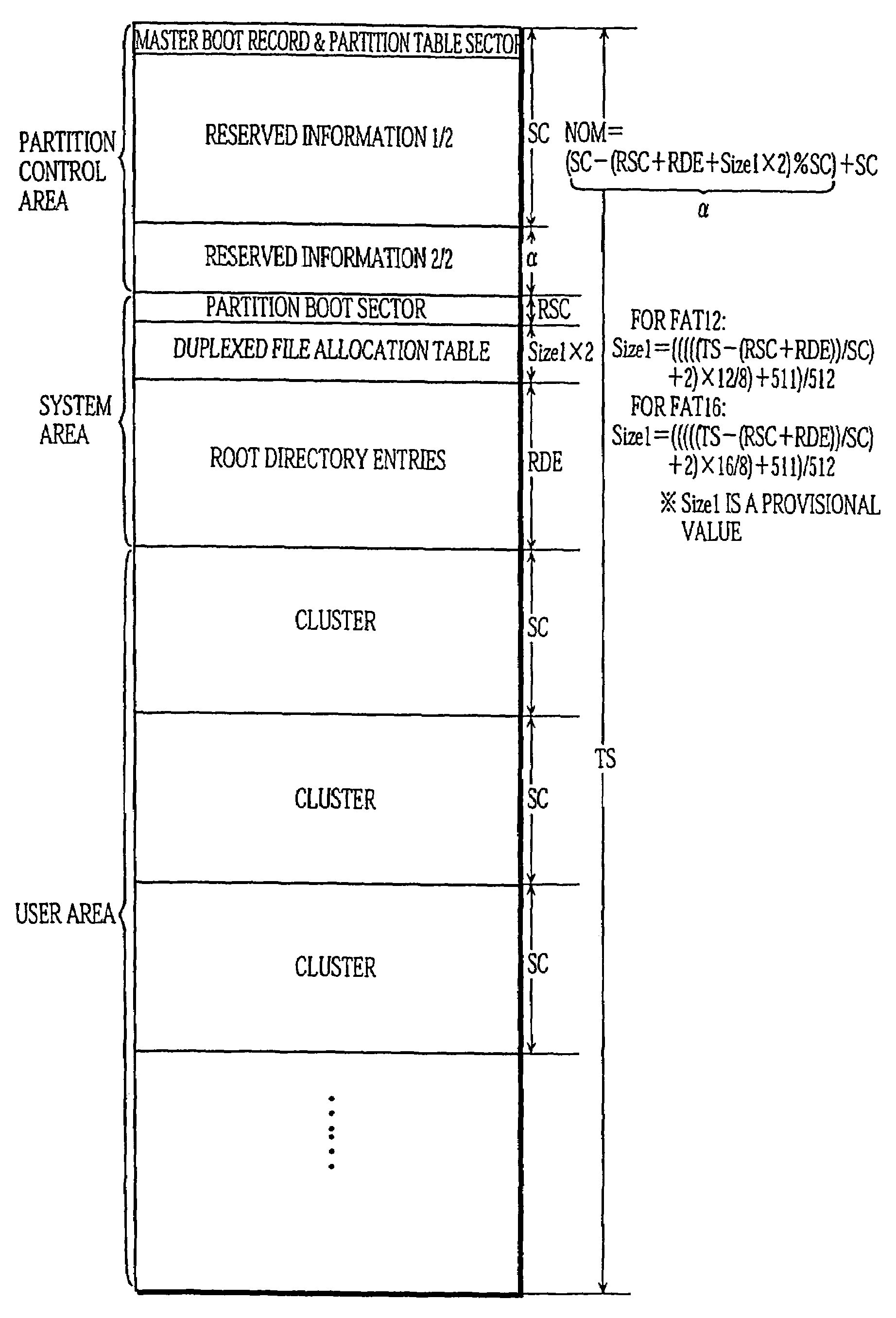
[0121]A second embodiment proposes an arrangement in which the volume area is divided into an area to which the general user can gain access (the user data area), and an area that stores data securely (the protected area).

[0122]A structure of an access apparatus 200 and a semiconductor memory card 100 in the second embodiment are shown in FIG. 14. In the internal structure shown in the drawing, in contrast to that shown in FIG. 3A, the nonvolatile memory 1 has been provided with a protected area, and the semiconductor memory card 100 and the access apparatus 200 have been provided respectively with secure processing units 11 and 12.

[0123]The following is an explanation of the secure processing unit 11 provided in order to perform secure reading and writing to and from the protected area in the nonvolatile memory 1. As shown in FIG. 15, the secure processing unit 11 includes a system area 13, a hidden area 14, an AKE processing unit 15, a Ks decrypting unit 16, and a Ks encrypting un...

third embodiment

[0155]The third embodiment relates to an improvement used when data stored in erasable blocks is erased, the erasable blocks being managed using a logical address and a physical address. A structure of an access control unit 2 in the third embodiment is shown in FIG. 19. The access control unit 2 in the drawing includes a command decoding unit 21, a logical / physical address conversion unit 22, a read control unit 23, an allocation changing unit 24, a write control unit 25, an erase control unit 26, and a modify control unit 27.

[0156]The command decoding unit 21 receives a command issued by an access apparatus 200, and decodes the original content of the command at the point of issue. If a read command is received, the command decoding unit 21 instructs the read control unit 23 to read data from the nonvolatile memory 1 (Read). If a write command is received, the command decoding unit 21 instructs the write control unit 25 to write data into the nonvolatile memory 1 (Write). If a wri...

fourth embodiment

[0176]The fourth embodiment describes an improvement realized when the processing of the third embodiment is performed using an erased block table instead of an erased block list. FIG. 24 shows an internal structure for an access apparatus 2002 in the fourth embodiment. If this drawing is compared with FIG. 19, it can be seen that the erased block list has been replaced by an erased block table. The erased block table in the fourth embodiment is formed from entries corresponding to each erasable block. If a block is erased, the corresponding entry is set at ‘1’ and if a block is unerased, the corresponding entry is set at ‘0’. The erased block table expresses the erase state of each erasable block by setting either ‘1’ or ‘0’ in the erased block table.

[0177]As a result of the erased block list having been replaced by the erased block table, the processing performed by the write control unit 25 and the erase control unit 26 in the fourth embodiment differs from that performed in the ...


PUM

PropertyMeasurementUnit
timeaaaaaaaaaa
timeaaaaaaaaaa
sizeaaaaaaaaaa

Abstract

A predetermined number of erasable blocks positioned at a start of a volume area in a semiconductor memory card are provided so as to include volume management information. A user area following the volume management information includes a plurality of clusters. A data length NOM of an area from a master boot record & partition table sector to a partition boot sector is determined so that the plurality of clusters in the user area are not arranged so as to straddle erasable block boundaries. Since cluster boundaries and erasable block boundaries in the user area are aligned, there is no need to perform wasteful processing in which two erasable blocks are erased to rewrite one cluster.

Description

[0001]This application is a divisional application of U.S. patent application Ser. No. 10 / 444,966, filed May 27, 2003, now U.S. Pat. No. 6,829,674, which is a divisional application of U.S. patent application Ser. No. 09 / 691,269, filed Oct. 19, 2000, now U.S. Pat. No. 6,611,907.[0002]This application is based on an application No. 11-299636 filed in Japan, the content of which is hereby incorporated by reference.BACKGROUND OF THE INVENTION[0003]1. Field of the Invention[0004]The present invention relates to an access apparatus for accessing a semiconductor memory card having internal nonvolatile memory such as EEPROM (electrical erasable programmable read-only memory), a computer-readable recording medium for recording an initialization program for a semiconductor memory card, an initialization method, and a semiconductor memory card, and in particular to an improvement for raising the efficiency with which data can be rewritten in the nonvolatile memory.[0005]2. Description of the ...

Claims


Application Information

Patent Timeline
Patent Type & Authority Patents(United States)
IPC IPC(8): G06F12/00G06F12/14G06F3/06G06F12/02G06F21/60G06F21/62G06F21/79G11B20/00G11B20/12
CPCG06F3/0613G06F3/0616G06F3/064G06F3/0643G06F3/0652G06F3/0679G06F3/0644G06F12/1433G06F12/0223G06F12/0246G06F2212/1016G06F2212/2022G06F2212/7202G11B20/00086
Inventor MAEDA, TAKUJIHIROTA, TERUTO
Owner PANASONIC CORP
Why Eureka
Try Eureka