Zero capacitance bondpad utilizing active negative capacitance

a negative capacitance, active technology, applied in the direction of radiation controlled devices, semiconductor devices, semiconductor/solid-state device details, etc., can solve the problems of reducing the reliability of the circuit, reducing the performance of the circuit, and high cost of the layer structure modification, so as to reduce the capacitance of the bondpad of the integrated circuit, effectively eliminating the bondpad capacitance, and the effect of negative capacitan

Active Publication Date: 2006-12-12
BELL SEMICON LLC
View PDF10 Cites 4 Cited by
  • Summary
  • Abstract
  • Description
  • Claims
  • Application Information

AI Technical Summary

Benefits of technology

[0006]Accordingly, the present invention is directed to an apparatus and system for reducing bondpad capacitance of an integrated circuit. In an embodiment of the invention, circuitry of the present invention may produce a negative capacitance approximately equal in magnitude to the capacitance associated with the bondpad and thereby effectively eliminate the bondpad capacitance. Further, circuitry of the present invention may be employed within an integrated circuit without modifying the layer structure of the integrated circuit. In an advantageous aspect of the present invention, values of the components of the circuitry may be selectively and independently chosen to synthesize a variable range of negative capacitance. Thus, the circuitry of the present invention may be employed in a variety of integrated circuits, each of which may have a unique capacitance associated with the bondpad.

Problems solved by technology

A drawback caused by the capacitance associated with the bondpad 180 is a reduction in circuit performance.
However, modification of the layer structure is expensive and typically causes reduced reliability of the circuit.
Further, this type of capacitance reduction only provides a minimal reduction in capacitance.

Method used


Image

  • Zero capacitance bondpad utilizing active negative capacitance
  • Zero capacitance bondpad utilizing active negative capacitance
  • Zero capacitance bondpad utilizing active negative capacitance

Examples


Embodiment Construction

[0014]Reference will now be made in detail to the presently preferred embodiments of the invention, examples of which are illustrated in the accompanying drawings.

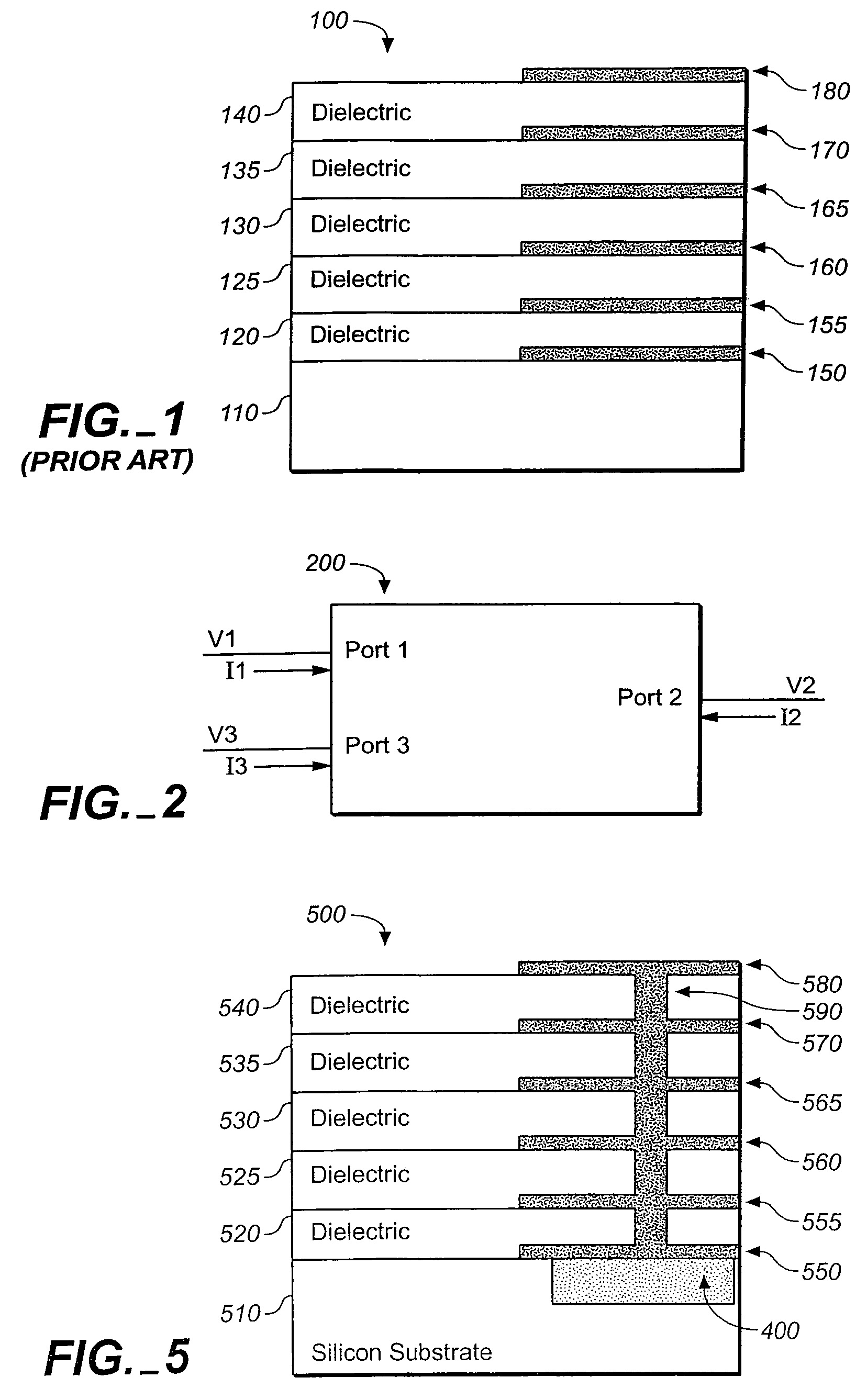
[0015]Referring to FIG. 2, an embodiment of a current conveyor 200 in accordance with the present invention is shown. Current conveyor 200, a three port device, may be the building block of a negative capacitance generator (shown in FIG. 3) of the present invention, with the following properties:

[0016][i1i2v3]=[0000-10100]⁡[v1i3v3](Equation⁢⁢1)

[0017]From Equation 1, the following equations may be obtained:

i1=0

i2=−i3

v3=v1

[0018]From these equations, it may be determined that the current conveyor 200 has a high impedance node at Port 1, in which there may be no current flow. Current conveyor 200 may also have a voltage follower property that may transfer the voltage at Port 1 to Port 3 along with a current flow property that may transfer current from Port 3 through Port 1.

[0019]Referring to FIG. 3, an embodiment of a negative...


PUM


Abstract

The present invention is an apparatus and system for reducing bondpad capacitance of an integrated circuit. Circuitry of the present invention may produce a negative capacitance approximately equal in magnitude to the capacitance associated with the bondpad and thereby effectively eliminate the bondpad capacitance. Values of the components of the circuitry may be selectively and independently chosen to synthesize a variable range of negative capacitance and thus produce a negative capacitance approximately equal in magnitude to a unique capacitance associated with the bondpad of a variety of integrated circuits.

Description

FIELD OF THE INVENTION[0001]The present invention generally relates to the field of integrated circuits, and more particularly to an apparatus for reducing bondpad capacitance of an integrated circuit.BACKGROUND OF THE INVENTION[0002]Integrated circuits are employed in most of the digital appliances utilized on a daily basis by consumers. Integrated circuits may refer to an electronic circuit built onto a single piece of substrate, a chip, and enclosed within a package. Integrated circuits generally perform a desired function or plurality of functions. In the fabrication of integrated circuits, bondpads are employed to form the connection from the integrated circuit to the package. A package may refer to the housing of the chip and electrically interconnects the chip with outside circuitry.[0003]Referring to FIG. 1, an embodiment of an integrated circuit 100 known to the art is shown. An integrated circuit 100 may include a silicon substrate layer 110 with multiple dielectric layers...

Claims


Application Information

Patent Timeline
Patent Type & Authority Patents(United States)
IPC IPC(8): H01L23/48H01L23/485H01L23/52H01L23/522
CPCH01L23/5222H01L24/05H01L2924/1305H01L2924/00014H01L2924/01033H01L2224/05599H01L2924/01006H01L2924/01014H01L2924/13091H01L2924/14H01L2924/19041H01L2924/19043H01L2924/30105H01L2924/3011H01L2924/00
Inventor SINGH, PRASHANT K.
Owner BELL SEMICON LLC
Why Eureka
Try Eureka