Memory devices with buffered command address bus

a command address and memory module technology, applied in memory adressing/allocation/relocation, instruments, climate sustainability, etc., can solve the problems of reducing the bandwidth of the command address bus, reducing and reducing the efficiency of the dram-based memory device. , to achieve the effect of reducing the bandwidth reducing the overloading of the command address bus, and increasing the number of memory modules

Inactive Publication Date: 2006-12-12
ROUND ROCK RES LLC
View PDF16 Cites 53 Cited by
  • Summary
  • Abstract
  • Description
  • Claims
  • Application Information

AI Technical Summary

Benefits of technology

[0011]It is an object of this invention to increase the number of memory modules and the number of ranks of memory devices connectable to

Problems solved by technology

Inefficiencies in DRAM-based memory devices arise when successive accesses are made to different rows in the same internal bank.
Such accesses cause the currently open row to be closed before a different row can be opened, thus delaying the access.
However, closing rows immediately after access can still result in an unnecessary delay should the next access be to the same row (because now that same row has to be re-opened).
Because multi-rank memory modules include memory devices connected in parallel, a potentially large number of memory devices use the same signals, which can resul

Method used


Image

  • Memory devices with buffered command address bus
  • Memory devices with buffered command address bus
  • Memory devices with buffered command address bus

Examples


Embodiment Construction

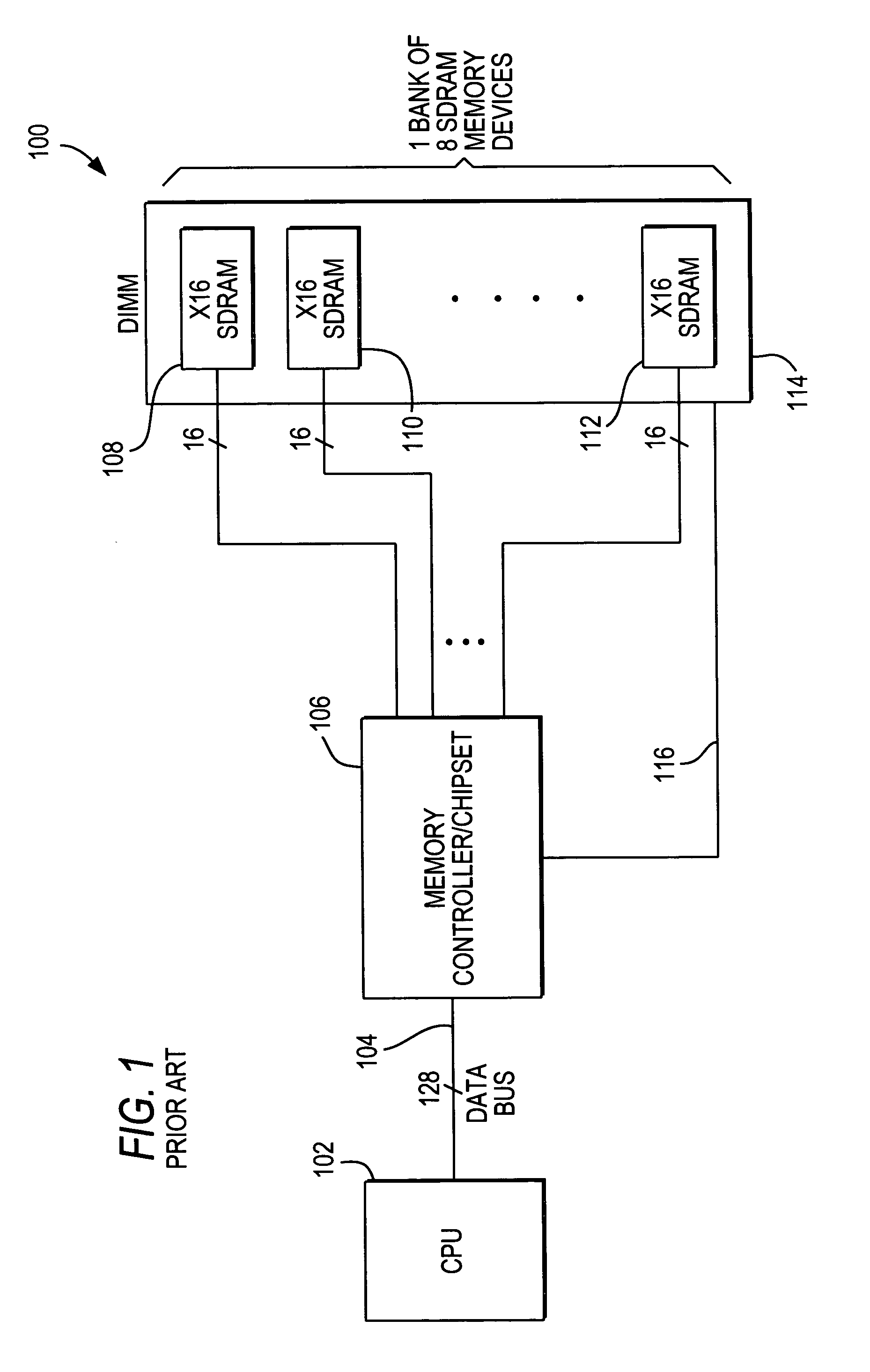
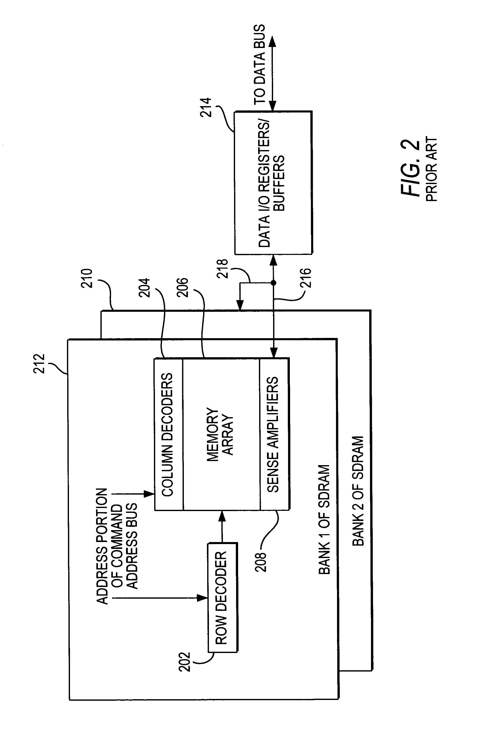
[0024]SDRAM-based memory modules (including DDR (double data rate) SDRAM-based devices) and other types of memory modules that have multiple ranks advantageously can increase memory access throughput by having many activated internal banks and rows in each rank. Memory access schemes are known and can be developed that take advantage of this parallel activation of more than one rank of memory devices.

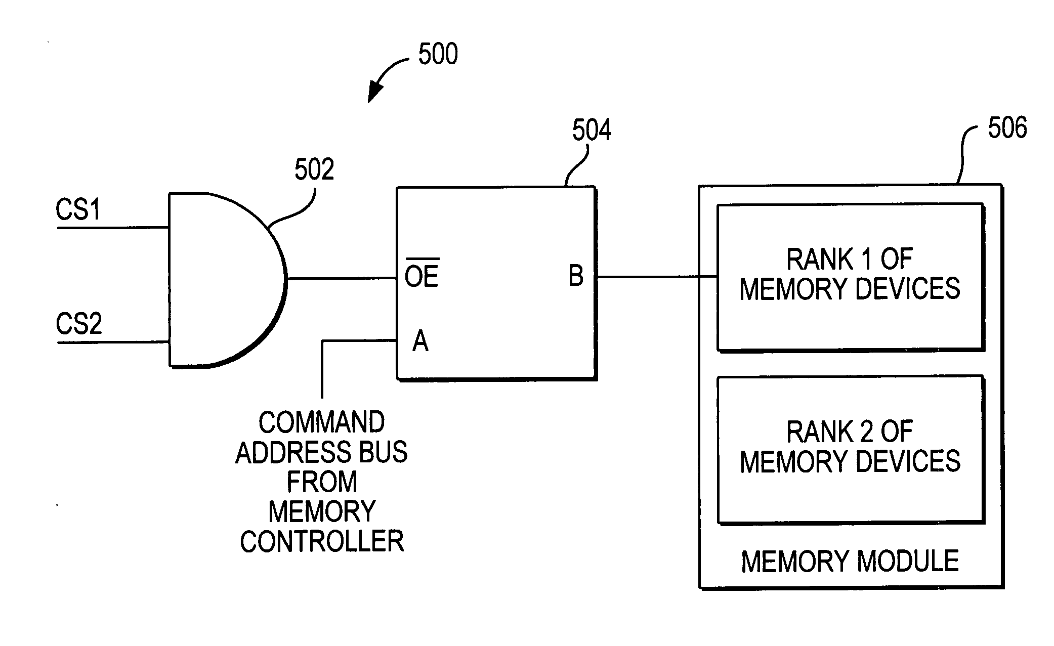
[0025]However, because a high number of ranks of memory devices can result in signal degradation on the command is address bus shared between these ranks, the command address bus is advantageously connected to switches between the memory controller and the memory modules in accordance with the invention. The switches electrically isolate the command address bus from the ranks of memory devices. Each rank can be individually selected using a corresponding chip select signal, which also can be used to control the switches. Electrical overloading of the command address bus is reduced becau...


PUM


Abstract

Circuits and methods are provided that alleviate overloading of the command address bus and limit decreases in command address bus bandwidth to allow increased numbers of memory modules to be included in a computer system. A plurality of switches is coupled between the command address bus (which is coupled to the memory controller) and a respective plurality of memory modules. Each switch provides command address bus data only to its respective memory module. Preferably, only one switch does so at a time, limiting the loading seen by the memory controller.

Description

BACKGROUND OF THE INVENTION [0001]This invention relates to memory modules having multiple memory devices. More particularly, this invention relates to memory modules having multiple memory devices with reduced signal loading at the devices' interface.[0002]Computer systems are often designed to provide flexible memory resources (e.g., 512 megabytes, 1.2 gigabytes, etc.), and these memory resources can be designed with different combinations of memory modules, memory devices, or both. For example, the memory capacity of a computer system can be made up of one or more DRAM (dynamic random access memory) based memory modules. If a system's memory comprises two memory modules of equal size, each module represents half the system's memory capacity. One memory module can represent the “lower” half of the computer system's memory, and the other can represent the “upper” half. Alternatively, every other n-bytes of data can be stored in one memory module, while the remaining n-bytes of data...

Claims


Application Information

Patent Timeline
IPC IPC(8): G06F12/00G06F13/40G06F13/42G11C5/00
CPCG06F13/4022G06F13/4243G11C5/04Y02B60/1235Y02B60/1228Y02D10/00
Inventor LABERGE, PAUL A
Owner ROUND ROCK RES LLC
Why Eureka
Try Eureka