Determining wafer orientation in spectral imaging

a technology of spectral imaging and wafer orientation, applied in the direction of optical radiation measurement, instruments, spectrometry/spectrophotometry/monochromators, etc., can solve the problems of affecting the efficiency of semiconductor fabrication, requiring substantial space in the semiconductor fabrication cleanroom, and the system is too slow to be used concurrently with semiconductor processing,

Inactive Publication Date: 2006-12-19
FILMETRICS
View PDF5 Cites 31 Cited by
  • Summary
  • Abstract
  • Description
  • Claims
  • Application Information

AI Technical Summary

Problems solved by technology

Because the areas covered by these features are generally unsuitable for measurement of film properties, specific measurement sites called “pads” are provided at various locations on the wafer.
This small pad size presents a challenge for the film measurement equipment, both in measurement spot size and in locating the measurement pads on the large patterned wafer.
This is because current systems that measure thickness on patterned wafers are slow, complex, expensive, and require substantial space in the semiconductor fabrication cleanroom.
Such systems are too slow to be used concurrently with semiconductor processing, so the rate of semiconductor processing must be slowed down to permit film monitoring.
The result is a reduced throughput of semiconductor processing and hence higher cost.
Because the resolution and speed of available CCD imagers are limited, higher magnification sub-images of the wafer are required to resolve the measurement pads.
These additional sub-images require more time to acquire and also require complex moving lens systems and mechanical translation equipment.
The result is a questionable advantage in speed and performance over traditional microscope / pattern recognition-based spectral reflectance systems.
With spectral imaging techniques, the problem is similar, except that the imaging device and the reflectance measurement apparatus are the same, and the reflectance spectra are taken from the image in software after the pattern recognition step has determined the wafer orientation.
A problem in employing the methods described above is that images taken of nominally identical patterns on a wafer can vary greatly depending upon the film thicknesses present.
When the image contrast of the wafer changes such that shapes and edges invert or disappear, the software can no longer reliably determine wafer orientation.
Thus, pattern recognition software that relies on edge and / or shape detection can be ineffective or unreliable during wafer processing.

Method used


Image

  • Determining wafer orientation in spectral imaging
  • Determining wafer orientation in spectral imaging
  • Determining wafer orientation in spectral imaging

Examples


examples

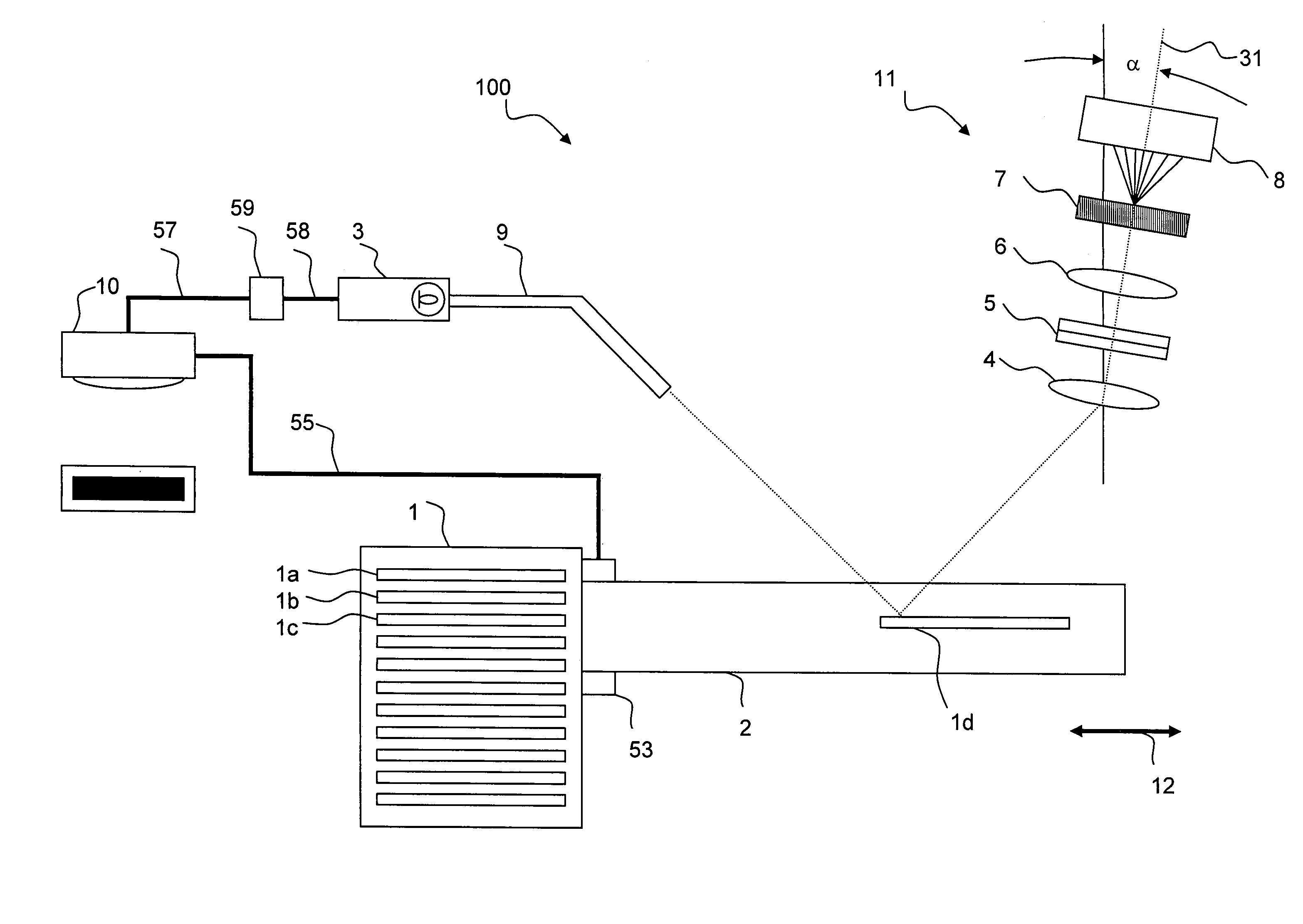
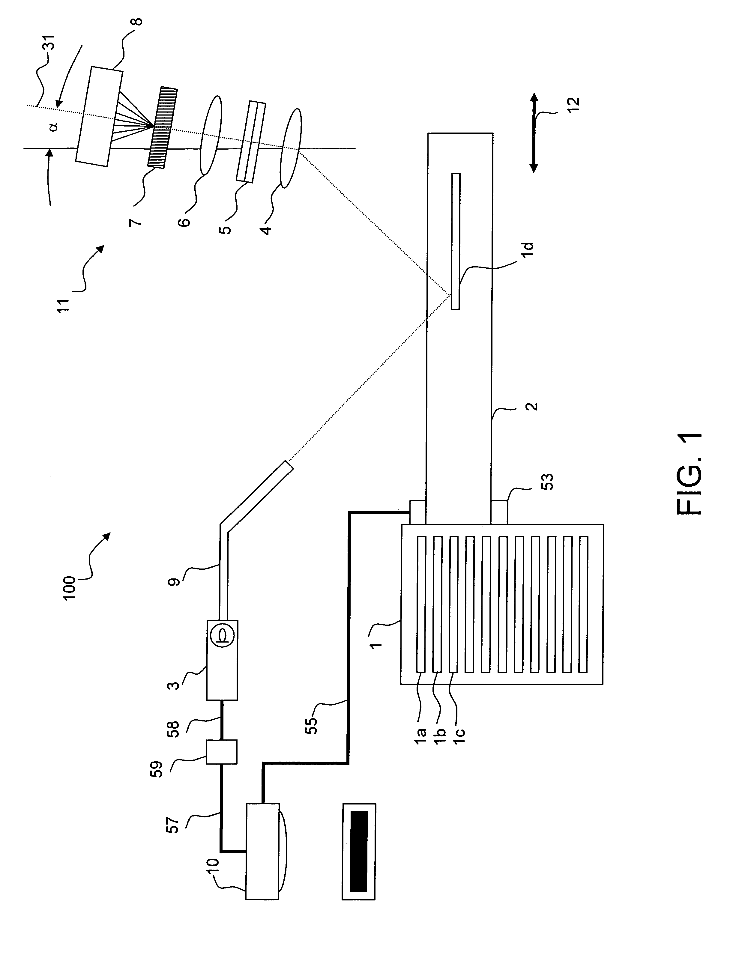
[0095]In an example embodiment, suitable for use in a CVD environment, the light source 3 is a tungsten / halogen regulated light source, manufactured by Stocker & Yale, Inc. (Salem, N.H.).

[0096]Fiber / fiber bundle 9 in this embodiment is a bundle configured into a line of fibers to provide uniform illumination along the measured surface. Several companies, Stocker & Yale being a prime example, manufacture such a fiber optic “line light”.

[0097]This example is configured for use with CVD processing system Model P5000 manufactured by Applied Materials Inc., Santa Clara, Calif. An optically clear viewport 18 is provided in the standard P5000 configuration.

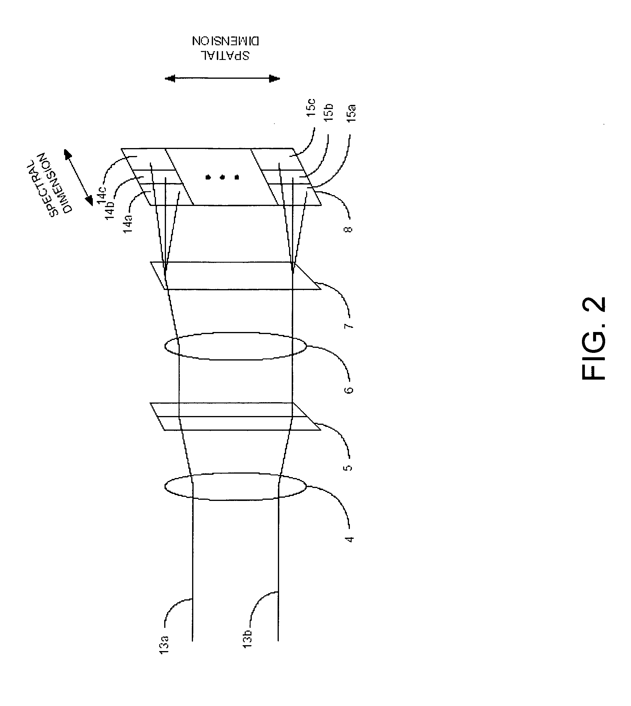
[0098]The line imaging spectrometer 11 in this example is manufactured by Filmetrics, Inc., San Diego, Calif., the assignee of the subject application. In this spectrometer, the imager 8 is a CCD imager incorporating a time delay and integration line scan camera manufactured by Dalsa Inc., Part No. CT-E4-2048 that has a CCD imager with 2...


PUM


Abstract

Devices and methods for determining wafer orientation in spectral imaging are described. The devices and methods generate an image of a wafer that includes at least one spectral dimension. One or more properties are determined from the spectral dimension, and a map is generated based on the property. The generated map is compared to at least one other map, and data or information of the comparison is used to locate a region of the wafer, for example a measurement pad or other structure.

Description

RELATED APPLICATIONS[0001]This application is a continuation-in-part of U.S. patent application Ser. No. 09 / 899,383, filed Jul. 3, 2001 now U.S. Pat. No. 7,095,511, which is a continuation-in-part of U.S. patent application Ser. No. 09 / 611,219, filed Jul. 6, 2000 now abandoned.[0002]This application claims the benefit of U.S. Patent Application No. 60 / 642,202, filed Jan. 7, 2005.[0003]This application is related to U.S. patent application Ser. No. 11 / 056,350, filed Feb. 10, 2005, and U.S. patent application Ser. No. 11 / 065,182, filed Feb. 23, 2005.FIELD[0004]This invention relates generally to the field of semiconductor film metrology, and, more specifically, to the field of film measurement during semiconductor wafer fabrication and processing, for pattern recognition, and for determining film thickness and goodness-of-fit.BACKGROUND[0005]Many industrial processes require precise control of film thickness. In semiconductor processing, for example, a semiconductor wafer is fabricate...

Claims


Application Information

Patent Timeline
Patent Type & Authority Patents(United States)
IPC IPC(8): G01B11/28
CPCG01B11/0625G01B11/0641G01N2021/213
Inventor CHALMERS, SCOTT A.GEELS, RANDALL S.
Owner FILMETRICS
Why Eureka
Try Eureka