Optical waveguide device, optical and electrical elements combined device, method of driving the same, and electronic equipment using the same

a technology of optical waveguides and combined devices, applied in the direction of optical waveguide light guides, optical elements, instruments, etc., can solve the problem that the solution of mounting techniques using only a conventional electrical connection has reached the limi

Inactive Publication Date: 2006-12-19
CANON KK
View PDF24 Cites 5 Cited by
  • Summary
  • Abstract
  • Description
  • Claims
  • Application Information

AI Technical Summary

Benefits of technology

[0014]According to the present invention, there is provided an electronic equipment, characterized in that a high speed optical connection between electrical chips can be freely reconfigured by incorporating the optical and electrical elements combined device of the present invention, and connections among a plurality

Problems solved by technology

However, the mounting technique using only a conventional electrical connection has reached the limit in solution of the problems of transmission delays and crosstalk, reduction of the EMI (Electromagnetic Interference), and t

Method used


Image

  • Optical waveguide device, optical and electrical elements combined device, method of driving the same, and electronic equipment using the same
  • Optical waveguide device, optical and electrical elements combined device, method of driving the same, and electronic equipment using the same
  • Optical waveguide device, optical and electrical elements combined device, method of driving the same, and electronic equipment using the same

Examples


first embodiment

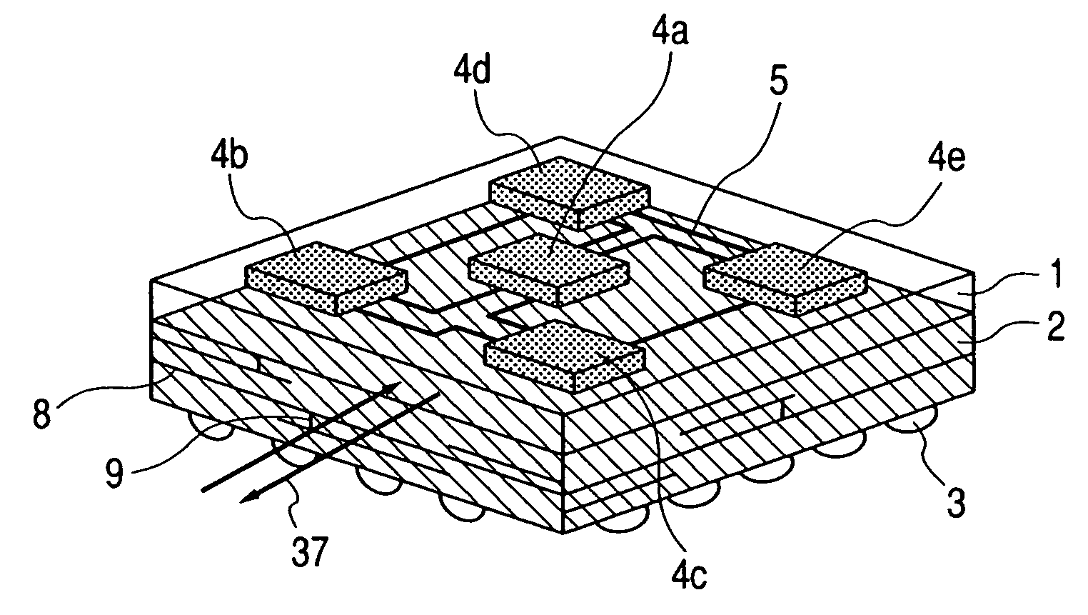
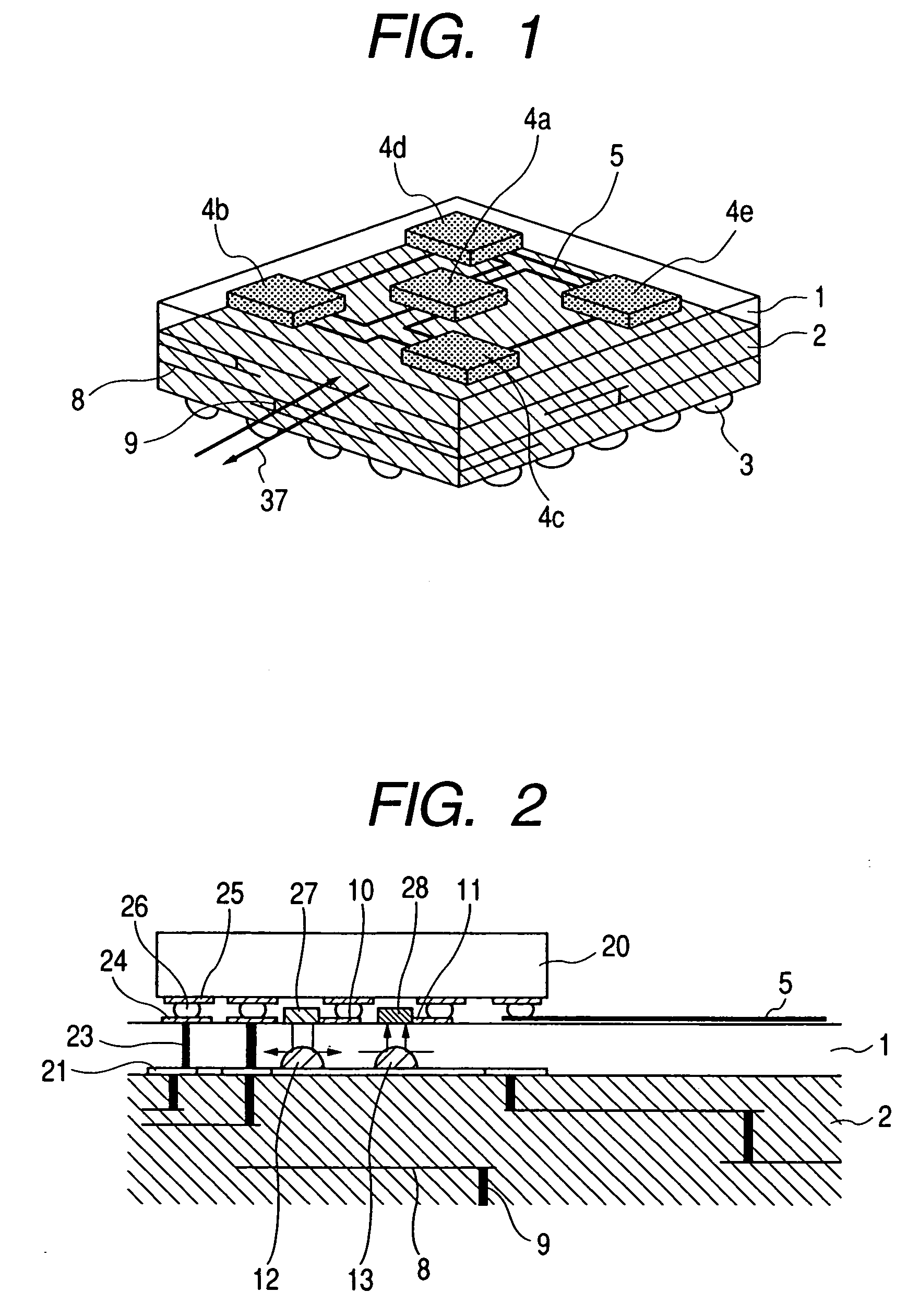
[0043]A perspective view of an optical and electrical elements combined device as a first embodiment of the present invention is shown in FIG. 1. In this embodiment, an optical waveguide layer 1 (slab type waveguide) which allows an optically free connection is laminated on a substrate 2 constituting a multilayer electrical wiring layer to be integrated with the substrate 2. In the form of FIG. 1, the optical waveguide layer 1 of a single layer is integrated on the uppermost surface. However, as will be described in subsequent embodiments as well, a form may also be adopted such that a multi-layered optical waveguide layer is integrated inside the electrical wiring layer.

[0044]As a material of the substrate 2 constituting the multi-layered electrical wiring layer, FR4 as constituting a printed substrate may be available. The following may also be available: an organic material such as a polyimide resin or an aramid resin; an inorganic ceramic material such as Al2O3 or AIN; glass; or...

second embodiment

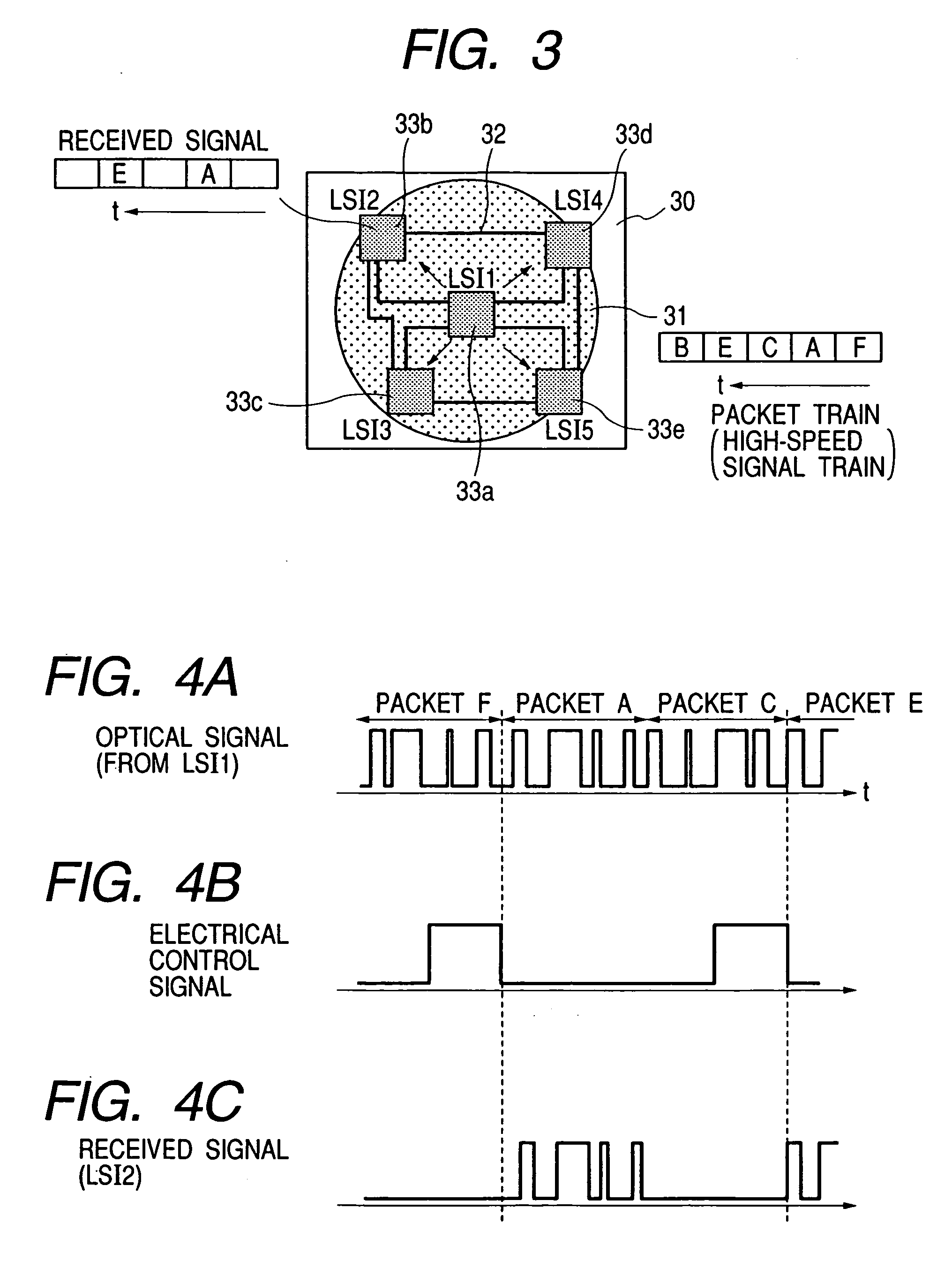
[0055]A second embodiment according to the present invention attains simultaneously transmitting signals from two or more chips. When as shown in FIGS. 6A to 6C, different signals are simultaneously transmitted from LSI chips 2 and 5, LSI chips 1, 3 and 4 each to be a reception chip must separately receive the optical signals. Then, as shown in FIGS. 6A to 6C, this is realized in such a way that the light intensities of the two optical signals are made different from each other, and the two optical signals are then processed in a reception circuit. The light intensity can be readily controlled if a current value for modulation of a laser is changed.

[0056]Assuming that for example, a light intensity of the chip 5 is Po; and a light intensity of the chip 2 is 2Po, if quantities of attenuation of the two optical signals received in the chip 1 are equal to each other at an equal distance, then the following combinations are offered.[0057]a) (chip 2, chip 5)=(0, 0)→received power; 0[0058...

third embodiment

[0062]A third embodiment according to the present invention is such that as shown in FIG. 7A, an optical waveguide layer 70 formed in a multi-layered structure is incorporated between electrical wiring layers 71 and 72. Unlike the first embodiment, this structure does not constitute a package, but constitutes a multichip module (MCM) realizing one function, and a size of the multichip module is in the range of about 50 mm to 100 mm square. While an interface with the outside is not illustrated, the multichip module is connected to the outside through a connector, an electrical cable, or an optical cable. All electrical wiring layers 71 and 72 including internal wirings 73 and 74, respectively, and an optical waveguide layer 70 are built-up, and LSIs 1 to 5 (75a to 75e), passive devices 76 and the like are compactly mounted on a surface of the electrical wiring layer 71.

[0063]The multi-layering of the optical waveguide layer 70 allows the mutual optical connections of a plurality of ...


PUM


Abstract

Disclosed is an optical waveguide device including an optical waveguide, and optical input and output ports for inputting and outputting an optical signal to and from the optical waveguide, characterized in that the optical input port receives an optical signal inputted from the optical output port to the optical waveguide in accordance with a timing control signal inputted as an electrical signal to the optical input port.

Description

[0001]This application is a continuation of International Application No. PCT / JP03 / 13699 filed on Oct. 27, 2003, which claims the benefit of Japanese Patent Application No. 2002-313733 filed on Oct. 29, 2002.BACKGROUND OF THE INVENTION[0002]1. Field of the Invention[0003]The present invention relates to an optical waveguide device including an optical waveguide and optical input and output ports for optically connecting a signal between electrical chips or the like within an electrical circuit substrate or a package, an optical and electronic elements combined device including the optical connection device and electrical circuits, a method of driving the optical and electrical elements combined device, and an electronic equipment using the optical and electrical elements combined device.[0004]2. Related Background Art[0005]In order to realize high performance of personal computers, mobile devices typified by cellular phones and PDAs (Personal Digital Assistants), digital AV (Audio V...

Claims


Application Information

Patent Timeline
IPC IPC(8): G02B6/12G02B6/42G02B6/122G02B6/43H01L31/12H04B10/00H04B10/40H04B10/50H04B10/524H04B10/60H04B10/80H05K1/02
CPCG02B6/12004H04B10/801G02B6/43G02B6/4214G02B6/4232
Inventor OUCHI, TOSHIHIKO
Owner CANON KK
Why Eureka
Try Eureka