Organic light emitting device having improved stability

a light-emitting diode and organic technology, applied in the direction of discharge tube luminescnet screens, instruments, natural mineral layered products, etc., can solve the problems of increasing the risk of operational degradation of the display, 80% of generated light is trapped within the device, and the small fraction of generated light available for viewing, etc., to achieve stable drive voltage, improve the stability of drive voltage, and improve the effect of top- or bottom emission efficiency

Active Publication Date: 2007-01-02
GLOBAL OLED TECH
View PDF13 Cites 22 Cited by
  • Summary
  • Abstract
  • Description
  • Claims
  • Application Information

AI Technical Summary

Benefits of technology

[0016]It is therefore an object of the present invention to provide top and bottom emitting microcavity OLEDs operable with stable drive voltage in long-term application.
[0017]It is another object of the present invention is to achieve the objects without compromising the lifetime or significantly affecting the efficiency of the device.
[0018]It is yet another object of the present invention is to achieve the objects without introducing significant complexity in the process or without major alteration of the device structure.
[0023](d) the reflective and conductive bilayer anode being configured to improve the stability of drive voltage.
[0024]In accordance with the present invention it was found that the bilayer anode structure including a base layer and a skin layer results in OLEDs, which exhibit stable drive voltage. In contrast to prior art OLEDs including a single layer metallic anode, the OLEDs of the present invention needs very little or no such adjustment in drive voltage, whereas in order to maintain drive current throughout the operating life the prior art device requires monotonic increase in drive voltage. It has been further determined that high efficiency of top- or bottom emission can be achieved by selecting a high reflectivity metallic base layer and a thin semitransparent skin alloy layer in the anode structure.

Problems solved by technology

However, only a small fraction of generated light is available for viewing, and about 80% of generated light is trapped within the device in waveguiding modes in glass, ITO and organic layers.
To compensate for the reduced average brightness level, the drive current has to be increased subjecting the display to increased risk of operational degradation.
It follows that more complex pixel drive circuitry cannot be readily implemented without further compromising aperture ratio and operation stability.
However, realizing high efficiency by reclaiming light lost to waveguiding modes can be very difficult.
To recover even a fraction of light lost to waveguiding modes the device architecture can be very complex.
It has been found, however, that the OLED based on the above layer structure was inefficient.
This is because the thin NPB can yield shorted OLEDs that can catastrophically fail in use.
On the other hand, thick NPB HTL is likely to increase the drive voltage.
In operation, OLEDs in general, degrade in performance characterized by loss of luminance with concurrent increase in drive voltage.
This provision results in wasted power even if the excess voltage is never used.
This would result in substantial saving in power consumption.

Method used


Image

  • Organic light emitting device having improved stability
  • Organic light emitting device having improved stability
  • Organic light emitting device having improved stability

Examples


example 1

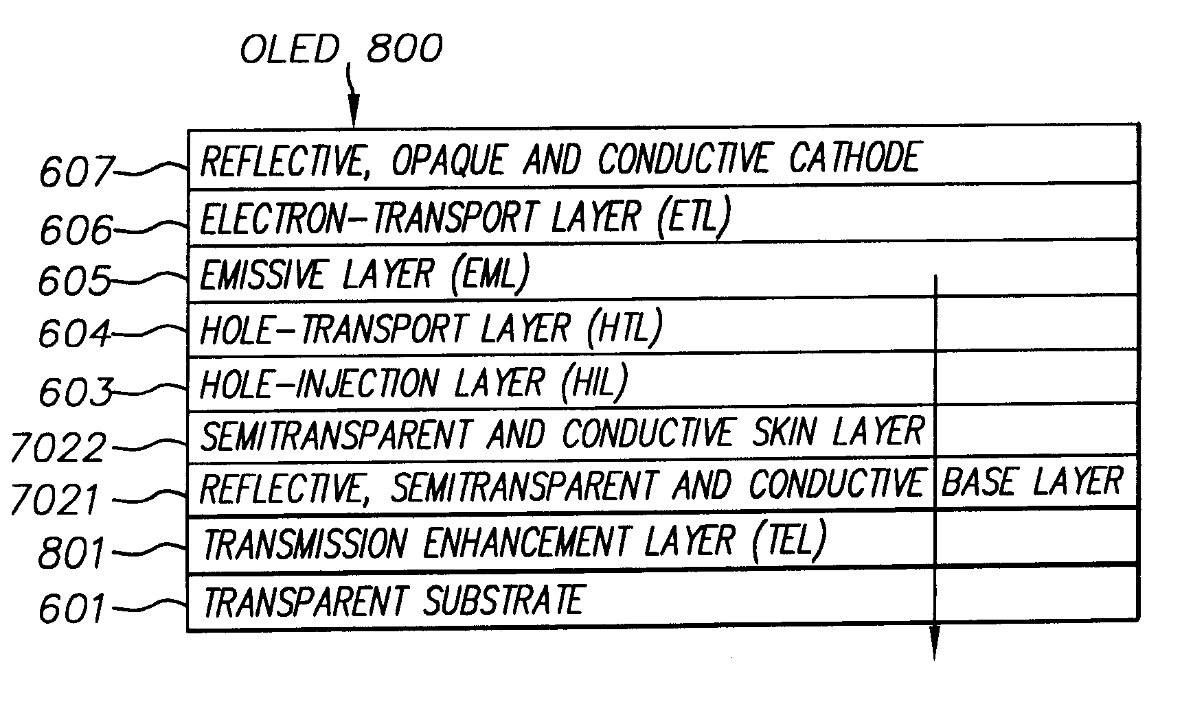
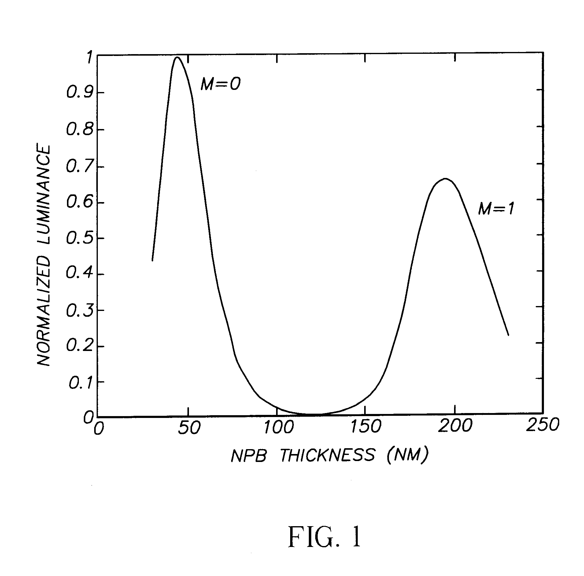
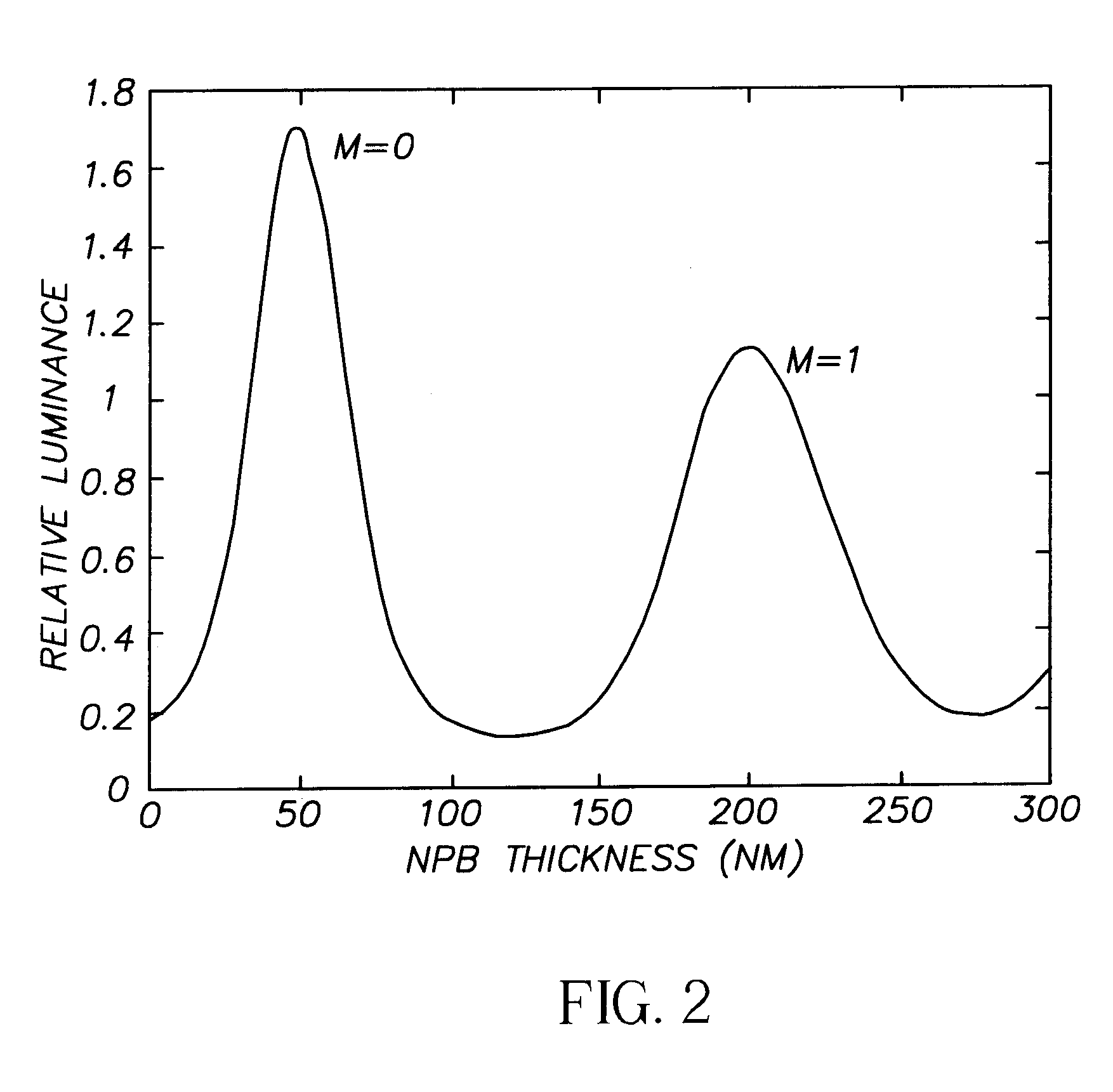
[0075]A prior art top-emitting device, OLED 1A and a top-emitting device, OLED 1B of the present invention were made in the same run. The prior art device was fabricated on glass substrate having a pure Ag anode, 60 nm thick, whereas the OLED of the present invention is a bilayer anode. The bilayer anode included a 60 nm thick base layer of pure Ag and a 6 nm thick skin layer of Ag Mo alloy. The concentration of Mo in the skin layer is 20% by volume. Each of the substrates was provided with a common CFx HIL, NPB HTL, Alq EML / ETL and a semitransparent top cathode. The cathode is an alloy, MgAg, semitransparent and 14 nm thick. The concentration of Ag in the cathode layer is 10% by volume. The OLED structures were selected based on the opaque, fully reflective and single layer anode of pure Ag and optimized for maximization of top emission. The devices have the following layer structures:[0076]OLED 1 A: Glass (1.1 mm) / Ag (60 nm) / CFx (1 nm) / NPB (45 nm) / Alq (60 nm) / MgAg (14 nm)[0077]OLE...

example 2

[0080]A prior art bottom-emitting device, OLED 2A, and a bottom-emitting device, OLED 2B of the present invention were made in the same coating run. The prior art OLED was fabricated on glass substrate having a pure Ag anode, semitransparent, and 20 nm thick, whereas the OLED of the present invention is a bilayer anode. The bilayer anode is also semitransparent and included a 15 nm thick base layer of pure Ag and a 6 nm thick skin layer of AgMo alloy. The concentration of Mo in the skin layer is 20% by volume. Each of the substrates was provided with a common CFx HIL, NPB HTL, Alq EML / ETL and a fully reflective top cathode. The cathode is an alloy, MgAg, opaque and 220 nm thick. The concentration of Ag in the cathode layer is 10% by volume. The OLED structures were selected based on the semitransparent, reflective and single layer anode of pure Ag and optimized for maximization of bottom emission. The devices have the following layer structures:[0081]OLED 2 A: Glass (1.1 mm) / Ag (20 ...

example 3

[0085]A prior art bottom-emitting device, OLED 3A, and a top-emitting device, OLED 3B of the present invention were made in the same coating run. The prior art OLED was fabricated on glass substrate having a pure Ag anode, semitransparent, and 20 nm thick, whereas the OLED of the present invention is a bilayer anode. The bilayer anode of the OLED of the present invention is opaque and included a 75 nm thick base layer of pure Ag and a 10 nm thick skin layer of AgMg alloy. The concentration of Mg in the skin layer is 50% by volume. Each of the substrates was provided with a common MoOx HIL, NPB HTL and an Alq EML / ETL. The cathode for the prior device, 3A, is a fully reflective LiF / Al layer, 100 nm thick. The cathode of the device 3B is an alloy, MgAg, semitransparent and 14 nm thick. The concentration of Ag in the cathode layer is 10% by volume. The devices have the following layer structures:[0086]OLED 3 A: Glass (1.1 mm) / Ag (20 nm) / MoOx (2 nm) / NPB (200 nm) / Alq (60 nm) / LiF (0.5 nm) / ...


PUM

PropertyMeasurementUnit
work functionaaaaaaaaaa
thicknessaaaaaaaaaa
thicknessaaaaaaaaaa

Abstract

In an OLED device, the improvement including a reflective and conductive bilayer anode including a metal or metal alloy or both; a hole-injecting structure over the reflective and conductive bilayer anode; at least one organic layer formed over the hole-injecting structure; and the reflective and conductive bilayer anode being configured to improve the stability of drive voltage.

Description

CROSS-REFERENCE TO RELATED APPLICATIONS[0001]Reference is made to commonly assigned U.S. patent application Ser. No. 10 / 347,013, filed Jan. 17, 2003, entitled “Organic Light Emitting Device (OLED) Display With Improved Light Emission Using a Metallic Anode” by Pranab K. Raychaudhuri et al.FIELD OF THE INVENTION[0002]The present invention relates to top- and bottom-emitting organic light emitting diodes (OLEDs), which use metallic electrodes and with improved stability in drive voltage which exhibit stable operational voltage in long-term use.BACKGROUND OF THE INVENTION[0003]An organic electroluminescent (OEL) device, alternately known as organic light emitting diode (OLED), is useful in flat-panel display applications. This light-emissive device is attractive because it can be designed to produce red, green, and blue colors with high luminance efficiency; it is operable with a low driving voltage of the order of a few volts and clearly viewable from oblique angles. These unique attr...

Claims


Application Information

Patent Timeline
Patent Type & Authority Patents(United States)
IPC IPC(8): H05B33/26H01L51/50H01L51/52
CPCH01L51/5206H01L51/5271Y10T428/24942Y10S428/917Y10T428/26H01L2251/5315H10K50/816H10K50/818H10K50/852H10K50/856H10K2102/3026H05B33/26
Inventor RAYCHAUDHURI, PRANAB K.MADATHIL, JOSEPH K.LIAO, LIANG-SHENG
Owner GLOBAL OLED TECH
Why Eureka
Try Eureka