Void free, silicon filled trenches in semiconductors

a technology of silicon filled trenches and semiconductors, applied in the field of semiconductor devices, can solve the problems of reducing the size of device components, challenging the balance of performance and other manufacturing constraints, and affecting the formation of inner electrodes of high aspect ratio trenches

Inactive Publication Date: 2007-01-02
POLARIS INNOVATIONS LTD
View PDF3 Cites 48 Cited by
  • Summary
  • Abstract
  • Description
  • Claims
  • Application Information

AI Technical Summary

Benefits of technology

[0012]One or more embodiments of the present invention provide methods of forming substantially void free trench structures in semiconductor devices. In accordance with one embodiment of the present invention, a method of fabricating a semiconductor device is provided. The method of this embodiment comprises forming a trench having sidewalls in a semiconductor substrate, depositing a layer of amorphous (a-Si) or polysilicon in the trench, and annealing the a-Si or polysilicon layer in a hydrogen atmosphere to collapse any voids in the trench. Preferably, the annealing avoids recrystallization of a-Si or polysilicon in the sidewalls. According to one or more embodiments, the trenches are high aspect ratio trenches, for examples trenches having an aspect ratio greater than about 20.

Problems solved by technology

Unfortunately, performance can suffer when device component size is reduced.
Therefore, it is a challenge to balance performance with other manufacturing constraints.
A high aspect ratio trench adversely impacts formation of the inner electrode.
However, this process typically creates voids, gaps or seams within a central portion of the inner electrode.
However, larger taper adversely affects the “effective” trench depth (i.e., the depth of the trench excluding the tapered portion).
Etching through the a-Si or poly-Si will typically result in exposure of the void.
However, large voids often cause problems such as poor depth control of the healing deposition process.
As such, the deposition of poly-Si within long voids running substantially the depth of the trench may not sufficiently heal the defect.

Method used


Image

  • Void free, silicon filled trenches in semiconductors
  • Void free, silicon filled trenches in semiconductors
  • Void free, silicon filled trenches in semiconductors

Examples


Embodiment Construction

[0023]It is to be appreciated that the various process parameters described herein (by way of example only, temperature, time and pressure) are approximations and may be varied, and certain steps may be performed in different order. Before describing several exemplary embodiments of the invention, it is to be understood that the invention is not limited to the details of construction or process steps set forth in the following description. The invention is capable of other embodiments and of being practiced or carried out in various ways.

[0024]Like reference numerals have been used whenever possible to designate like components in the various embodiments of the present invention. Thus, in certain embodiments, various components or features may be designated by different reference numerals, while similar components and features will be designated by the same reference numerals.

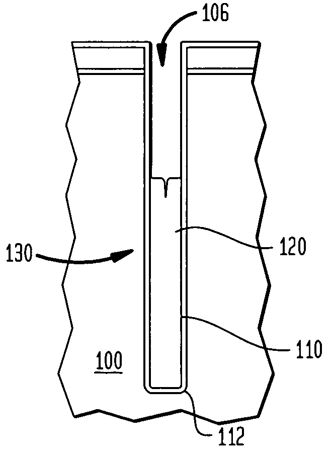
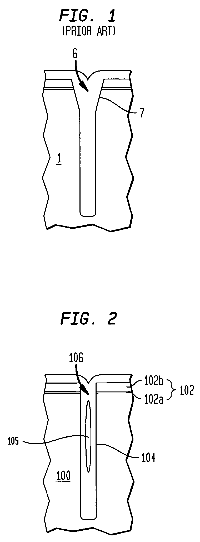
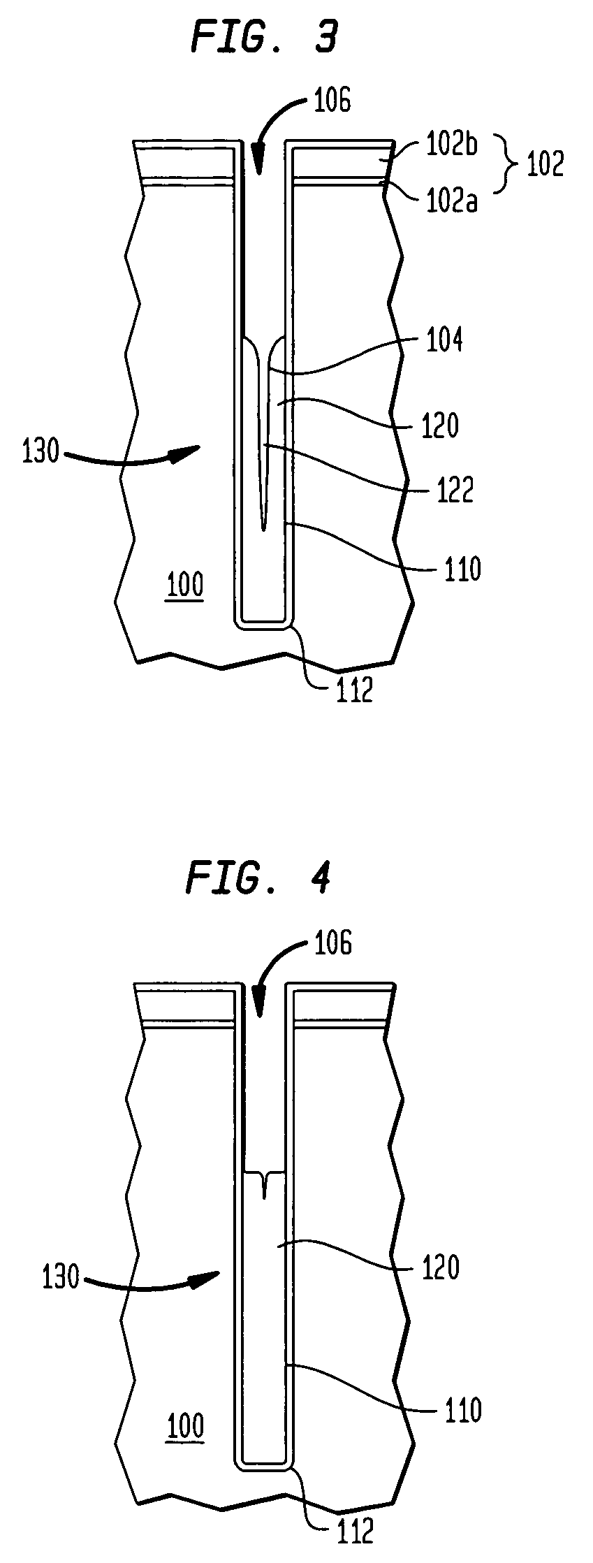
[0025]In accordance with an embodiment of the present invention, a method of producing substantially void-fr...


PUM

PropertyMeasurementUnit
temperatureaaaaaaaaaa
aspect ratioaaaaaaaaaa

Abstract

The present invention provides methods of producing substantially void-free trench structures. After deposition of an a-Si or polysilicon layer in a trench formed in a semiconductor, the a-Si or polysilicon is exposed to hydrogen at an elevated temperature.

Description

BACKGROUND OF THE INVENTION[0001]The present invention relates to semiconductor devices, and, more particularly, void-free, silicon filled trenches in semiconductors.[0002]Semiconductor devices are employed in various systems for a wide variety of applications. Device fabrication typically involves a series of process steps including layering materials on a semiconductor substrate wafer, patterning and etching one or more of the material layers, doping selected layers and cleaning the wafer.[0003]Semiconductor manufacturers continually seek new ways to improve performance, decrease cost and increase capacity of semiconductor devices. Capacity and cost improvements may be achieved by shrinking device size. For example, in the case of a dynamic random access memory (“DRAM”) chip, more memory cells can fit onto the chip by reducing the size of memory cell components such as capacitors and transistors. The size reduction results in greater memory capacity for the chip. Cost reduction is...

Claims


Application Information

Patent Timeline
Patent Type & Authority Patents(United States)
IPC IPC(8): H01L21/8242
CPCH01L29/66181H01L27/1087H01L21/763H01L21/2022H10B12/0387H01L21/02667H01L21/02532H01L21/02595
Inventor HAUPT, MORITZ
Owner POLARIS INNOVATIONS LTD
Why Eureka
Try Eureka