Method of mounting electronic component on substrate without generation of voids in bonding material

a technology of electronic components and bonding materials, which is applied in the direction of soldering media, printed circuit assembling, conductive pattern formation, etc., can solve the problems of failure of electric contact between electronic components and substrates, and achieve the effect of improving productivity

Inactive Publication Date: 2007-01-09
FUJITSU LTD
View PDF8 Cites 10 Cited by
  • Summary
  • Abstract
  • Description
  • Claims
  • Application Information

AI Technical Summary

Benefits of technology

[0006]It is accordingly an object of the present invention to provide a method of mounting an electronic component on a substrate, which is capable of enhancing the reliability of bonding between the electronic component and the substrate.

Problems solved by technology

The voids may cause a failure in electric contact between the electronic component and the substrate.

Method used


Image

  • Method of mounting electronic component on substrate without generation of voids in bonding material
  • Method of mounting electronic component on substrate without generation of voids in bonding material
  • Method of mounting electronic component on substrate without generation of voids in bonding material

Examples


Embodiment Construction

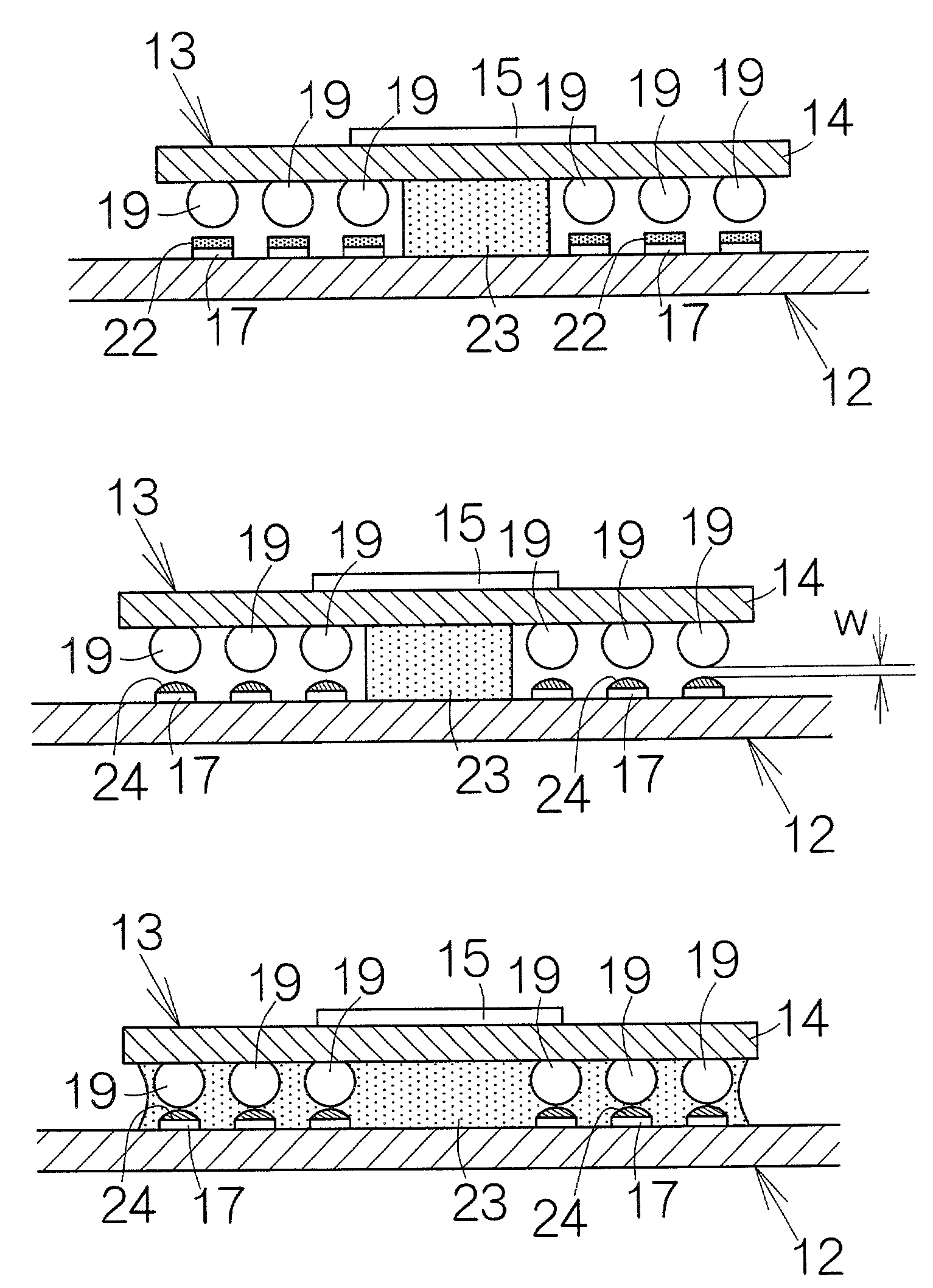
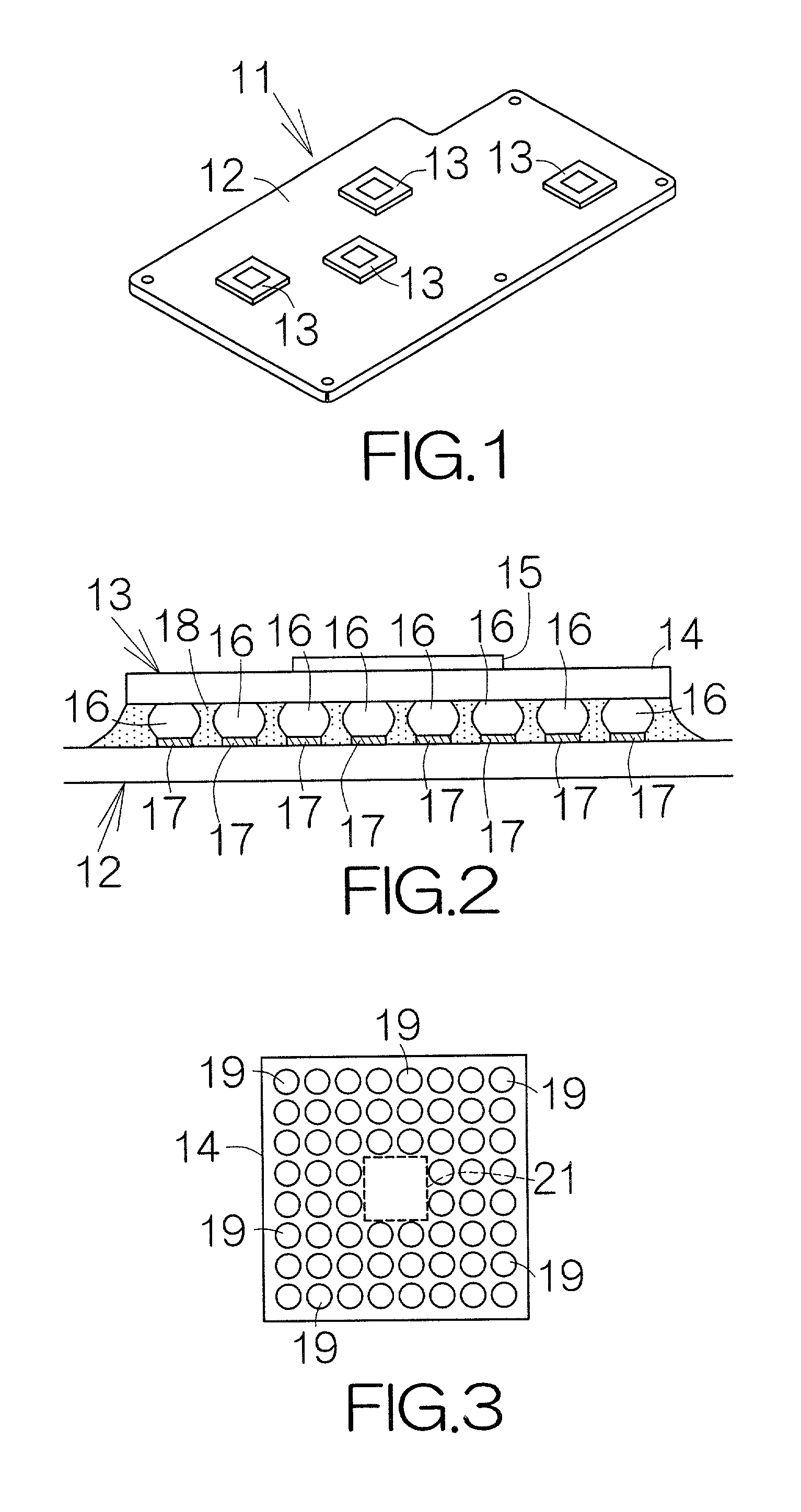
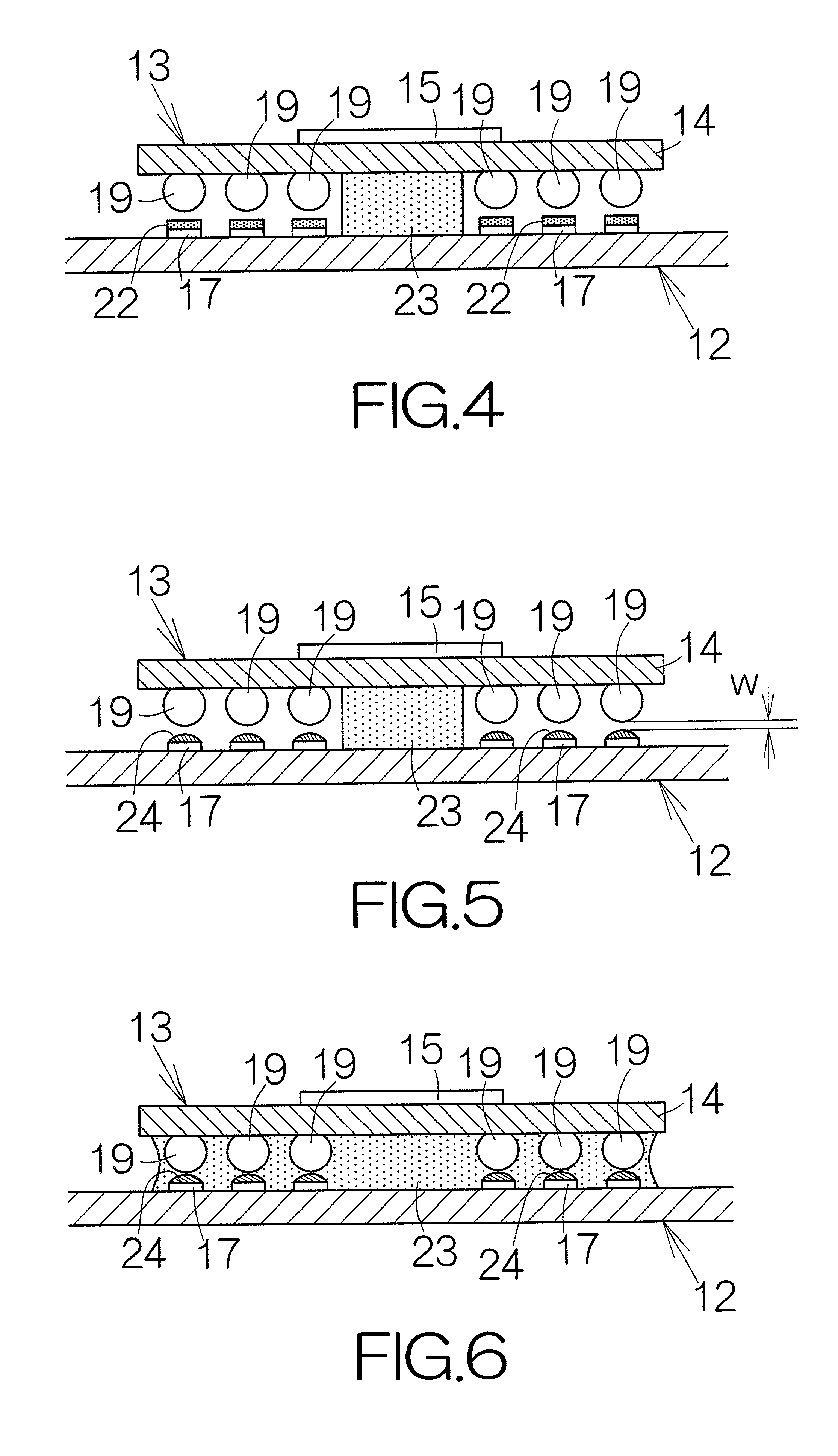
[0031]FIG. 1 schematically illustrates the structure of a electronic circuit board 11. The electronic circuit board 11 includes a printed wiring board or substrate 12 of a resin material, for example, and one or more electronic components 13, such as ball grid array (BGA) semiconductor packages, mounted on the surface of the printed wiring board 12. An electrically conductive wiring pattern, not shown, spreads over the surface or / and interior of the printed wiring board 12 so as to establish electric connections between the BGA semiconductor packages 13, for example.

[0032]As shown in FIG. 2, the BGA semiconductor package 13 includes a semiconductor chip 15 mounted on the upper surface of a small-sized printed wiring board or substrate 14 of a ceramic material, for example. A plurality of connection terminals 16 are attached to the lower surface of the small-sized printed wiring board 14. The connection terminals 16 are received on corresponding terminal pads 17 on the printed wiring...


PUM

PropertyMeasurementUnit
melting pointaaaaaaaaaa
temperatureaaaaaaaaaa

Abstract

When an electronic component is mounted on a substrate, the electronic component is first placed on the substrate with a solid support interposed between the electronic component and the substrate. The solid support serves to space a terminal conductor of the electronic component from a corresponding terminal pad on the substrate. A conductive bonding material is then melted on the terminal pad. The melted conductive bonding material gets exposed to the peripheral atmosphere over a larger area. Even if a bubble is generated within the melted conductive bonding material, the bubble is allowed to easily get out of the melted conductive bonding material. Removal of the gas is promoted in the melted conductive bonding material. The solid support is subsequently melted. The electronic component is moved down toward the substrate, thereby contacting the terminal conductor with the melted conductive bonding material on the corresponding terminal pad. Removal of the gas in this manner leads to improvement in the strength of bonding between the substrate and the electronic component.

Description

BACKGROUND OF THE INVENTION[0001]1. Field of the Invention[0002]The present invention relates to a method of mounting an electronic component, such as a ball grid array (BGA) semiconductor package. In particular, the invention relates to a method of mounting an electronic component on a substrate by melting a conductive bonding material on a terminal pad on the substrate.[0003]2. Description of the Prior Art[0004]Some methods of mounting an electronic component on a substrate utilize a solder paste. The solder paste is previously printed on terminal pads disposed on the surface of the substrate. Terminal conductors, such as solder balls, of the electronic component are placed on the corresponding terminal pads. After the electronic component has been set on the substrate in this manner, the substrate is passed through a reflow oven. Solder particles dispersed within the solder paste are caused to melt in the reflow oven. Subsequent cooling treatment serves to solidify the solder on ...

Claims


Application Information

Patent Timeline
Patent Type & Authority Patents(United States)
IPC IPC(8): H05K3/30H01L21/60H01L29/78H05K3/34
CPCH05K3/305H05K3/3436Y10T29/49144H05K3/3494H05K2201/0129H05K2201/10734H05K2201/10977H05K2203/0182H05K2203/0475H05K2203/1105H01L2224/29036Y10T29/49146Y10T29/49151Y10T29/4913Y10T29/49169Y10T29/49155Y10T29/49163H01L2224/29035H01L2224/73103H01L2224/73204Y02P70/50H01L2924/00012H01L29/78
Inventor YAMAMOTO, TSUYOSHISUEHIRO, MITSUOYAMADA, HIROSHI
Owner FUJITSU LTD
Why Eureka
Try Eureka