RF switching circuit for use in mobile communication systems

a mobile communication system and switching circuit technology, applied in electronic switching, pulse technique, semiconductor devices, etc., can solve the problems of waveform distortion, insufficient isolation to an rf signal, deterioration of rf characteristics at high power input, etc., to achieve excellent isolation, low harmonic distortion, and small size

Inactive Publication Date: 2007-01-09
COLLABO INNOVATIONS INC
View PDF2 Cites 71 Cited by
  • Summary
  • Abstract
  • Description
  • Claims
  • Application Information

AI Technical Summary

Benefits of technology

[0012]It is therefore an object of the present invention to provide a switching circuit in which deterioration of isolation and increase of harmonic distortion with respect to an RF signal are prevented and the insertion loss in an ON state is small even with the use of a multi-gate FET.

Problems solved by technology

However, the RF switches using FETs have a drawback in which their RF characteristics deteriorate at the input of high power.
As a result, the isolation to an RF signal becomes insufficient.
In a case where the depletion layers formed in regions under the gates expand insufficiently, the OFF state of the RF switching circuit is not maintained when a relatively-low signal is input, so that waveform distortion occurs.
As a result, there arises a problem in which this waveform distortion increases harmonic distortion.
In this case, however, in the ON state where the power supply voltage is applied to the gates, the potential difference between each of the gates and the source is 0 V and an insufficient forward bias voltage is generated.
Accordingly, there arises another problem of a large insertion loss in this ON state.

Method used


Image

  • RF switching circuit for use in mobile communication systems
  • RF switching circuit for use in mobile communication systems
  • RF switching circuit for use in mobile communication systems

Examples


embodiment 1

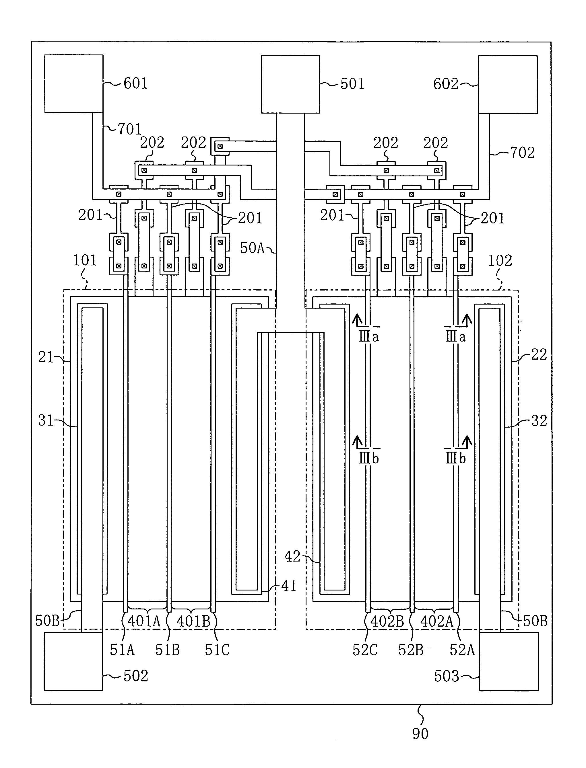
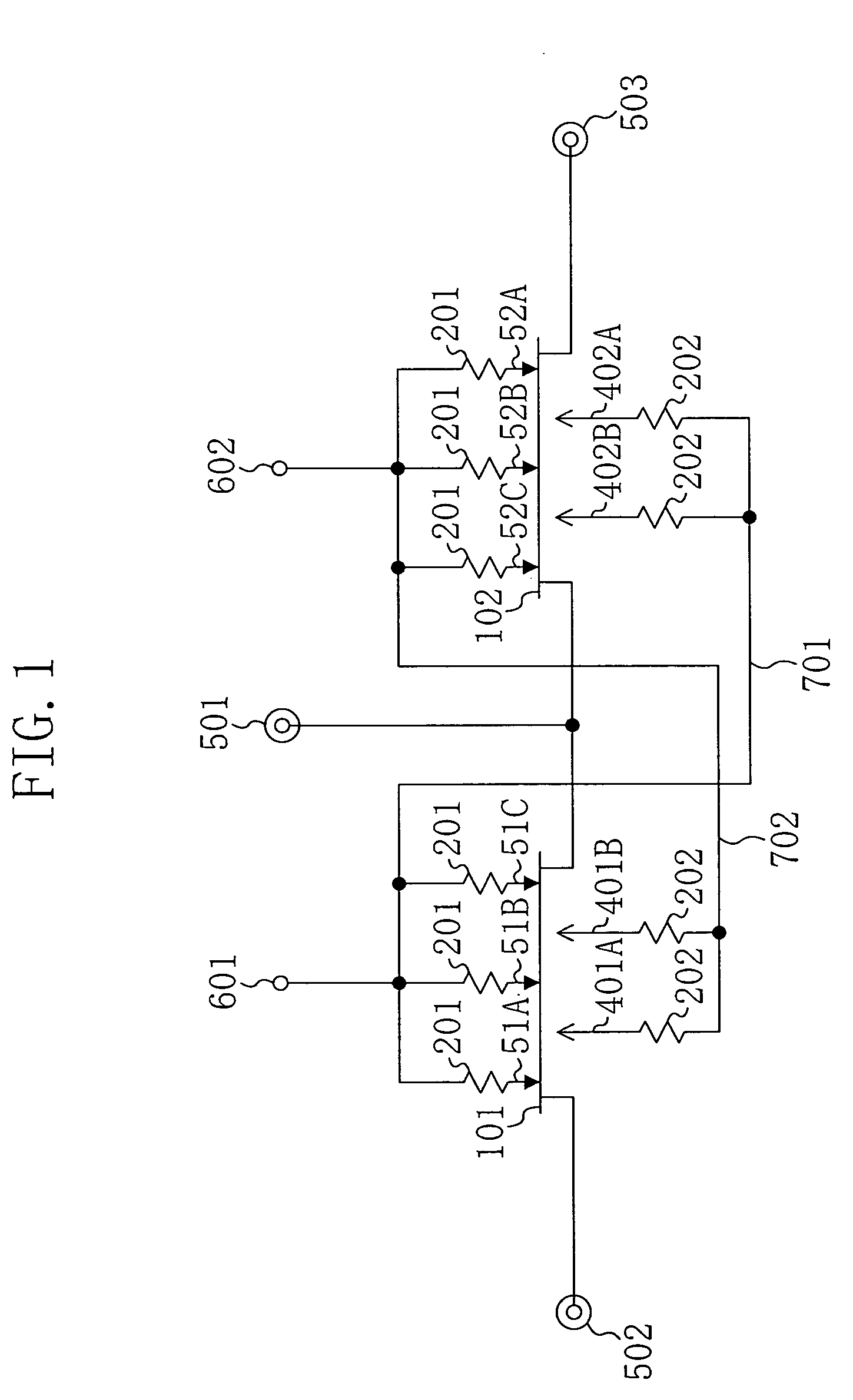
[0054]A first embodiment of the present invention will be described with reference to the drawings. FIG. 1 illustrates an equivalent circuit of an RF switching circuit according to the first embodiment. As shown in FIG. 1, a first FET 101, which is a multi-gate field effect transistor (FET) having three gates, is connected between a first input / output terminal 501 and a second input / output terminal 502. A second FET 102, which is also a multi-gate FET having three gates, is connected between the first input / output terminal 501 and a third input / output terminal 503. In this manner, a single pole double throw (SPDT) RF switching circuit is configured.

[0055]The first FET 101 has a first gate 51A, a second gate 51B and a third gate 51C that are connected to a first control line 701 via respective resistors 201. The second FET 102 has a first gate 52A, a second gate 52B and a third gate 52C that are connected to a second control line 702 via respective resistors 201.

[0056]On the other ha...

modified example 1 of embodiment 1

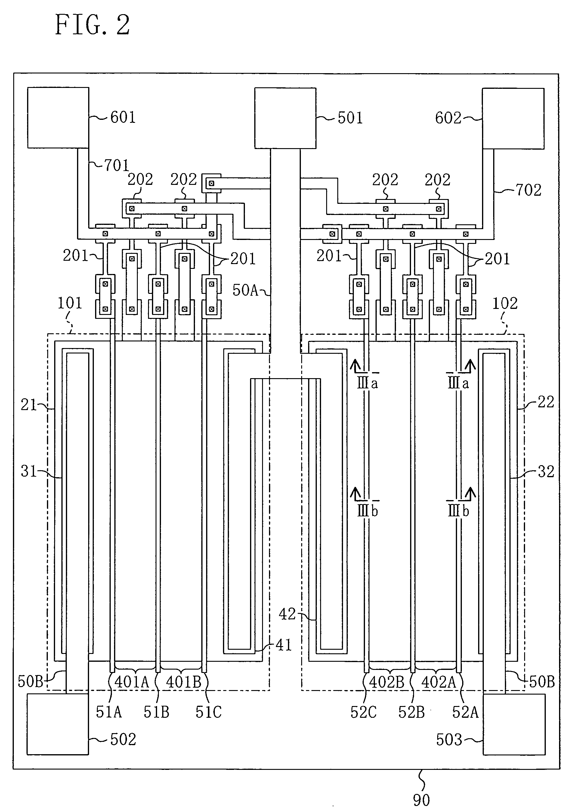
[0073]Hereinafter, a first modified example of the first embodiment will be described with reference to the drawings. FIG. 6 illustrates an equivalent circuit of an RF switching circuit according to this modified example. In FIG. 6, components already shown in FIG. 1 are denoted by the same reference numerals, and thus descriptions thereof will be omitted.

[0074]As shown in FIG. 6, in the RF switching circuit of this modified example, inter-gate regions 401A and 401B of a first FET 101 are connected to the cathodes of respective diodes 141 whose anodes are connected to a second control line 702 via respective resistors 202. In the same manner, inter-gate regions 402A and 402B of a second FET 102 are connected to the cathodes of respective diodes 141 whose anodes are connected to a first control line 701 via respective resistors 202.

[0075]In this modified example, when 0 V is applied to a second control terminal 602, for example, a forward current flowing from a first gate 51A to a th...

modified example 2 of embodiment 1

[0077]Hereinafter, a second modified example of the first embodiment will be described with reference to FIG. 7. FIG. 7 illustrates an equivalent circuit of an RF switching circuit according to this modified example. In FIG. 7, components already shown in FIG. 1 are denoted by the same reference numerals, and thus descriptions thereof will be omitted.

[0078]As shown in FIG. 7, in the RF switching circuit of this modified example, inter-gate regions 401A and 401B of a first FET 101 are connected to inter-gate regions 402A and 402B of a second FET 102 via resistors 202.

[0079]In the RF switching circuit of this modified example, in a case where an RF signal input to a second input / output terminal 502 is output from a first input / output terminal 501, for example, when the first FET 101 is turned ON and the second FET 102 is turned OFF, the potentials at the inter-gate regions 401A and 401B of the first FET 101 are increased by the applied RF signal. Accordingly, the potentials at the int...


PUM


Abstract

An RF switching circuit according to the present invention includes: a plurality of input / output terminals for inputting and outputting an RF signal; and a switch for opening and closing an electrical connection between the input / output terminals. The switch is constituted by a multi-gate field effect transistor including a plurality of gates located between source and drain spaced from each other on a semiconductor layer. A bias voltage is applied to an inter-gate region of the semiconductor layer between the gates. The bias voltage is equal to or lower than 90% of a high-level voltage, which is a voltage for turning the multi-gate field effect transistor ON, in a state where the multi-gate field effect transistor is ON, and is equal to or higher than 80% of the high-level voltage and equal to or lower than the high-level voltage in a state where the multi-gate field effect transistor is OFF.

Description

CROSS-REFERENCE TO RELATED APPLICATION[0001]The disclosure of Japanese Patent Application No. 2004-161222 filed on May 31, 2004 including specification, drawings and claims is incorporated herein by reference in its entirety.BACKGROUND OF THE INVENTION[0002]The present invention relates to switching circuits and semiconductor devices for switching signals in, for example, mobile communication equipment.[0003]In recent mobile communication systems typified by cellular phones, expectations for radio-frequency (RF) switches with high performance using field effect transistors (FETs) have been growing. However, the RF switches using FETs have a drawback in which their RF characteristics deteriorate at the input of high power. To eliminate this drawback, a technique of connecting a plurality of FETs in series has been adopted. In addition, to reduce the size and cost of a semiconductor chip, a technique of using a multi-gate FET including a plurality of gate electrodes between a drain el...

Claims


Application Information

Patent Timeline
Patent Type & Authority Patents(United States)
IPC IPC(8): H01L29/76H01L27/04H01L21/822H01L27/088H01L27/095H01L29/74H01L29/80H03K17/62H03K17/687H03K17/693
CPCH01L27/088H03K17/693H03K17/6871
Inventor NAKATSUKA, TADAYOSHIFUKUMOTO, SHINJI
Owner COLLABO INNOVATIONS INC
Why Eureka
Try Eureka