Semiconductor device

a technology of semiconductor integrated circuits and semiconductor components, applied in semiconductor devices, electronic switching, pulse techniques, etc., can solve the problems of increasing the cost of producing deteriorating isolation characteristics, and inability to increase the integration density of semiconductor integrated circuit components without extending the size of semiconductor integrated circuit components, etc., to achieve high integration density, deterioration of isolation characteristics, and high integration density

Inactive Publication Date: 2008-09-16
COLLABO INNOVATIONS INC
View PDF18 Cites 6 Cited by
  • Summary
  • Abstract
  • Description
  • Claims
  • Application Information

AI Technical Summary

Benefits of technology

[0025]A second object to the present invention is to provide a semiconductor device for restraining an increase of insertion loss and a deterioration of a isolation characteristic of a switch circuit resulting from parasitic inductance of gold wires.
[0037]Accordingly, the present invention can provide either the low-cost miniaturized semiconductor integrated circuit component including the semiconductor chip for processing the high frequency signal and the semiconductor chip for controlling the process, restraining the increase of insertion loss of the switch circuit and the deterioration of the isolation characteristic resulting from the parasitic inductance of gold wires, and having a high integration density, or the semiconductor integrated circuit component including the semiconductor chip for processing the high frequency signal and the semiconductor chip for controlling the process, reducing the insertion loss of the switch circuit, and improving the isolation characteristic. Thus, the practical value of the present invention is quite high.

Problems solved by technology

However, pluralities of switch elements, shunt elements and MIM capacitors are formed on the switch circuit semiconductor chip so that the area of the switch circuit semiconductor chip is enlarged, which causes an increase of the cost of producing the semiconductor integrated circuit component.
Therefore, parasitic inductance by the gold wires is largely affected so as to increase the insertion loss of the switch circuit, and the isolation characteristic is deteriorated.
In other words, the number of elements to be mounted on the switch circuit semiconductor chip is restricted by the area of the substrate on which the semiconductor chip is mounted so that the integration density of the semiconductor integrated circuit component cannot be increased without extending the size of the semiconductor integrated circuit component.
However, the insertion loss and the isolation arise from a solid-state value of the semiconductor such as an electrical conductivity and a dielectric constant, and the solid-state value has a breaking point.
Therefore, the solid-state value determines the limits of the insertion loss and the isolation so that the insertion loss of the switch circuit cannot be reduced further and the isolation characteristic cannot be improved further.
As a result, a small insertion loss as in metal and a high isolation as in air cannot be realized in the semiconductor.
However, this method cannot realize the reduction of insertion loss and the improvement of the isolation characteristic at the same time because the insertion loss and the isolation are in a tradeoff relationship.
However, the MEMS switch needs a micro space structure at a mechanical contact point so that a complicated manufacturing process for a space formation is required.
Additionally, since conditions for the space formation to manufacture the MEMS switch need to be the same as possible, designing a space between elements and an arrangement of elements equally as possible for each element is restricted.
Therefore, it is difficult to manufacture the semiconductor integrated circuit component only by using the MEMS switches.
This method also cannot realize a reduction in the insertion loss and improve the isolation characteristic.

Method used


Image

  • Semiconductor device
  • Semiconductor device
  • Semiconductor device

Examples


first embodiment

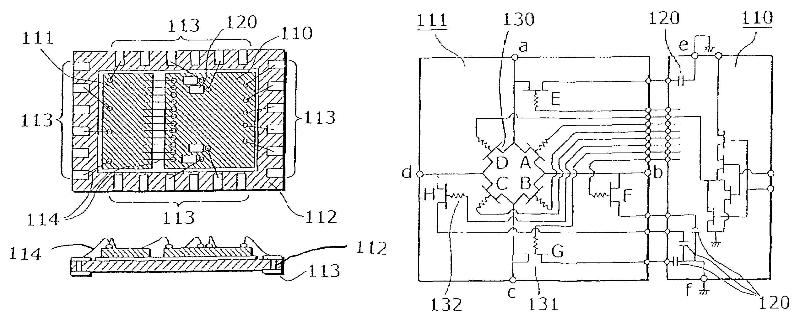
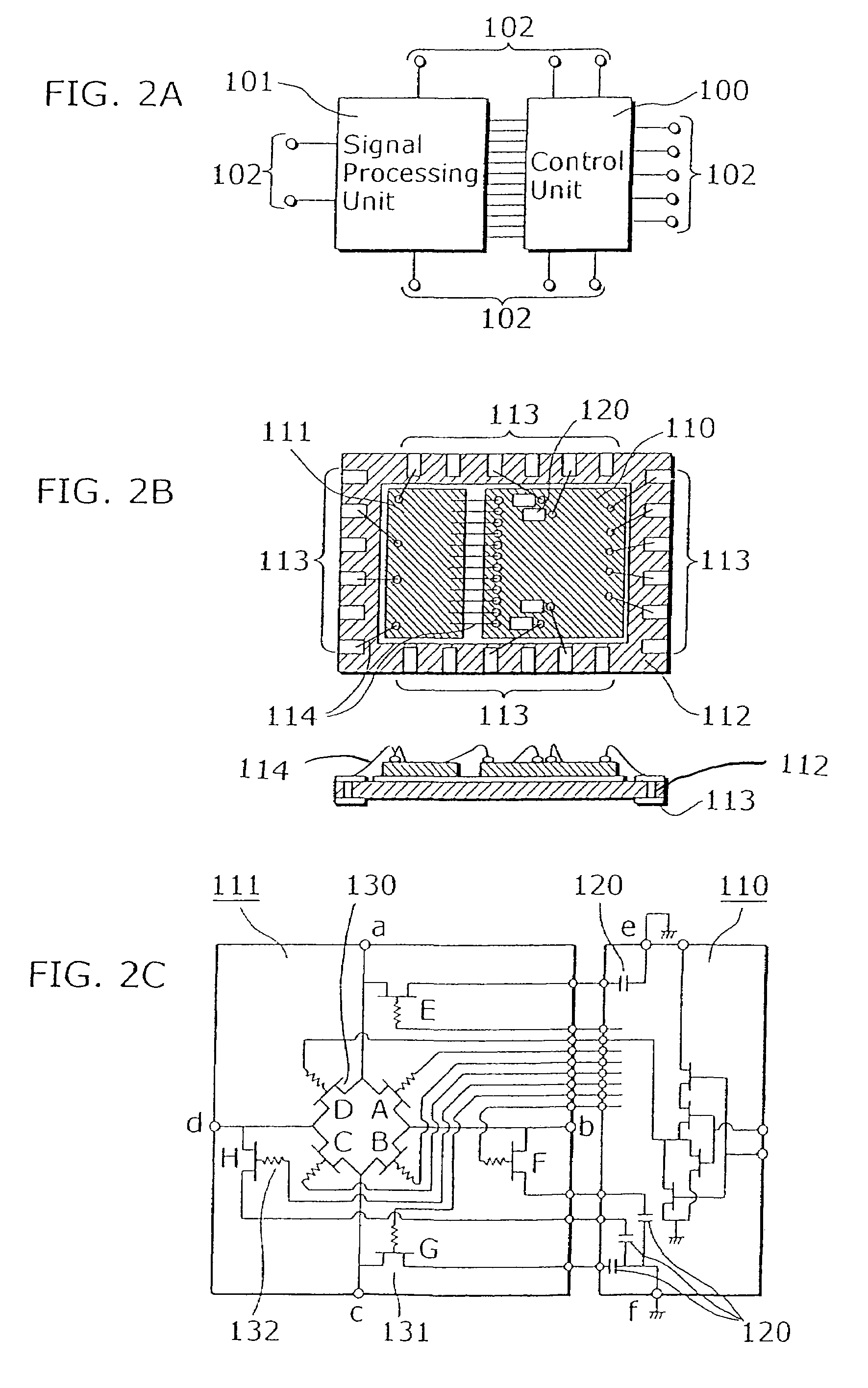
[0053]FIG. 2A is a functional block diagram showing an internal structure of a semiconductor integrated circuit component according to the first embodiment of the present invention.

[0054]The semiconductor integrated circuit component aims to realize a low-cost semiconductor integrated circuit component having a semiconductor chip for processing a high frequency signal and a semiconductor chip for controlling the high frequency signal processing. The semiconductor integrated circuit component is composed of a control unit 100, a signal processing unit 101 and terminals 102. The control unit 100 controls the signal processing unit 101 based on a signal inputted from the outside (i.e., an externally inputted signal). The signal processing unit 101 is connected to the control unit 100 and performs a switching operation of the high frequency signal. The terminals 102 are interfaces between the control unit 100 and the signal processing unit 101, and the outside.

[0055]FIG. 2B is an extern...

second embodiment

[0069]FIG. 3 is an external drawing of a semiconductor integrated circuit component according to the second embodiment of the present invention. In FIG. 3, the same elements as in FIG. 2B are denoted with the same reference numerals as in FIG. 2B and a detailed explanation thereof is omitted here.

[0070]The semiconductor integrated circuit component of the second embodiment aims to realize a semiconductor integrated circuit component for restraining an increase of the insertion loss and a deterioration of the isolation characteristic of a switch circuit resulting from the parasitic inductance of gold wires. While not mounting the control semiconductor chip and the switch circuit semiconductor chip next to each other on the substrate, the semiconductor integrated circuit component of the second invention differs from the semiconductor integrated circuit component of the first embodiment in that the control semiconductor chip is mounted on a substrate and the switch circuit semiconduct...

third embodiment

[0076]FIG. 5A is an external drawing of a semiconductor integrated circuit component according to the third embodiment of the present invention. In FIG. 5A, the same components as in FIG. 3 are denoted with the same reference numerals as in FIG. 3 and a detailed explanation thereof is omitted here.

[0077]The semiconductor integrated circuit component of the third embodiment aims to realize a miniaturized semiconductor integrated circuit component with a high integration density. The semiconductor integrated circuit component of the third embodiment differs with the semiconductor integrated circuit component of the second embodiment in that the switch circuit further includes the MIM capacitors, and the MIM capacitors are formed inside the substrate. The semiconductor integrated circuit component of the third embodiment is composed of the control semiconductor chip 110, a switch circuit semiconductor chip 111, a substrate 410, external terminals 113 and gold wires 210. Here, the subst...


PUM


Abstract

The present invention provides a miniaturized semiconductor device at low-cost having high integration density and for restraining an increase of an insertion loss and a deterioration of an isolation characteristic of a circuit resulting from parasitic inductance of gold wires. The semiconductor device includes a control semiconductor chip, a switch circuit semiconductor chip, a substrate, external terminals, gold wires and MIM capacitors. The control semiconductor chip controls a high frequency signal processing by the switch circuit semiconductor chip 111. The switch circuit semiconductor chip is mounted on the control semiconductor chip and processes the high frequency signal. The control semiconductor chip is mounted on the substrate. The external terminals are interfaces with the outside. The gold wires connect among the control semiconductor chip, the switch circuit semiconductor chip and the external terminals. The MIM capacitors are formed on the control semiconductor chip and the inside of the substrate, and process the high frequency signal.

Description

BACKGROUND OF THE INVENTION[0001](1) Field of the Invention[0002]The present invention relates to a semiconductor device. In particular, the present invention relates to a semiconductor integrated circuit component that is used for a communication device, a radio equipment and the like.[0003](2) Description of the Related Art[0004]In recent years, a high frequency signal is mostly used for the communication device and the radio equipment, and a field effect transistor (hereafter referred to as FET) using gallium arsenide (hereafter referred to as GaAs) which has a good high frequency characteristic is used for a switch circuit of the semiconductor integrated circuit component included in the communication device and the radio equipment.[0005]FIG. 1A is a functional block diagram showing an internal structure of the conventional semiconductor integrated circuit component (refer to Japanese Laid-Open Patent Publication application No. 11-144012).[0006]The semiconductor integrated circ...

Claims


Application Information

Patent Timeline
Patent Type & Authority Patents(United States)
IPC IPC(8): H01L29/76H01L25/04H01L25/065H01L25/07H01L25/18H03K17/56
CPCH01L25/18H01L2924/3011H01L2924/3025H01L2924/30107H01L2224/49175H01L2224/49171H01L2224/48227H01L2224/48137H01L2224/48091H01L2224/45144H01L2924/00014H01L2924/00H01L2224/48145H01L2924/00012H01L25/04
Inventor WATANABE, ATSUSHITARA, KATSUSHIHIDAKA, KENICHI
Owner COLLABO INNOVATIONS INC
Why Eureka
Try Eureka