Supercharge Your Innovation With Domain-Expert AI Agents!

Method for programming a memory arrangement and programmed memory arrangement

a memory arrangement and programming method technology, applied in the direction of digital storage, electrical appliances, instruments, etc., to achieve the effect of avoiding crosstalk between bit lines

Active Publication Date: 2007-01-09
INFINEON TECH AG
View PDF10 Cites 2 Cited by
  • Summary
  • Abstract
  • Description
  • Claims
  • Application Information

AI Technical Summary

Benefits of technology

The invention provides a memory arrangement with transistors and potential lines. The transistors have contacts that are connected to bit lines and potential lines for programming in different memory states. In one memory state, the contacts are connected to both the bit lines and the potential lines, while in the other memory state, the contacts are only connected to the potential lines. This arrangement helps to reduce capacitance between the bit lines and reduces crosstalk between memory cells. The transistors can be arranged in a matrix with address lines and bit lines, and several potential lines can be provided to shield the bit lines from each other. The potential line can be a virtual line or a negative supply voltage. The method for programming the memory cells involves connecting one of the contacts to a bit line and the other contact to the potential line for the first memory state, and no connections for the second memory state. This arrangement helps to improve the functioning and compactness of the memory arrangement.

Problems solved by technology

The ROM shown in FIG. 3 and 4 has the disadvantage that couplings can occur between individual memory cells or the bit lines, so that when a “1” is read, an adjacent programmed “0” can influence the read result.

Method used


Image

  • Method for programming a memory arrangement and programmed memory arrangement
  • Method for programming a memory arrangement and programmed memory arrangement
  • Method for programming a memory arrangement and programmed memory arrangement

Examples


Embodiment Construction

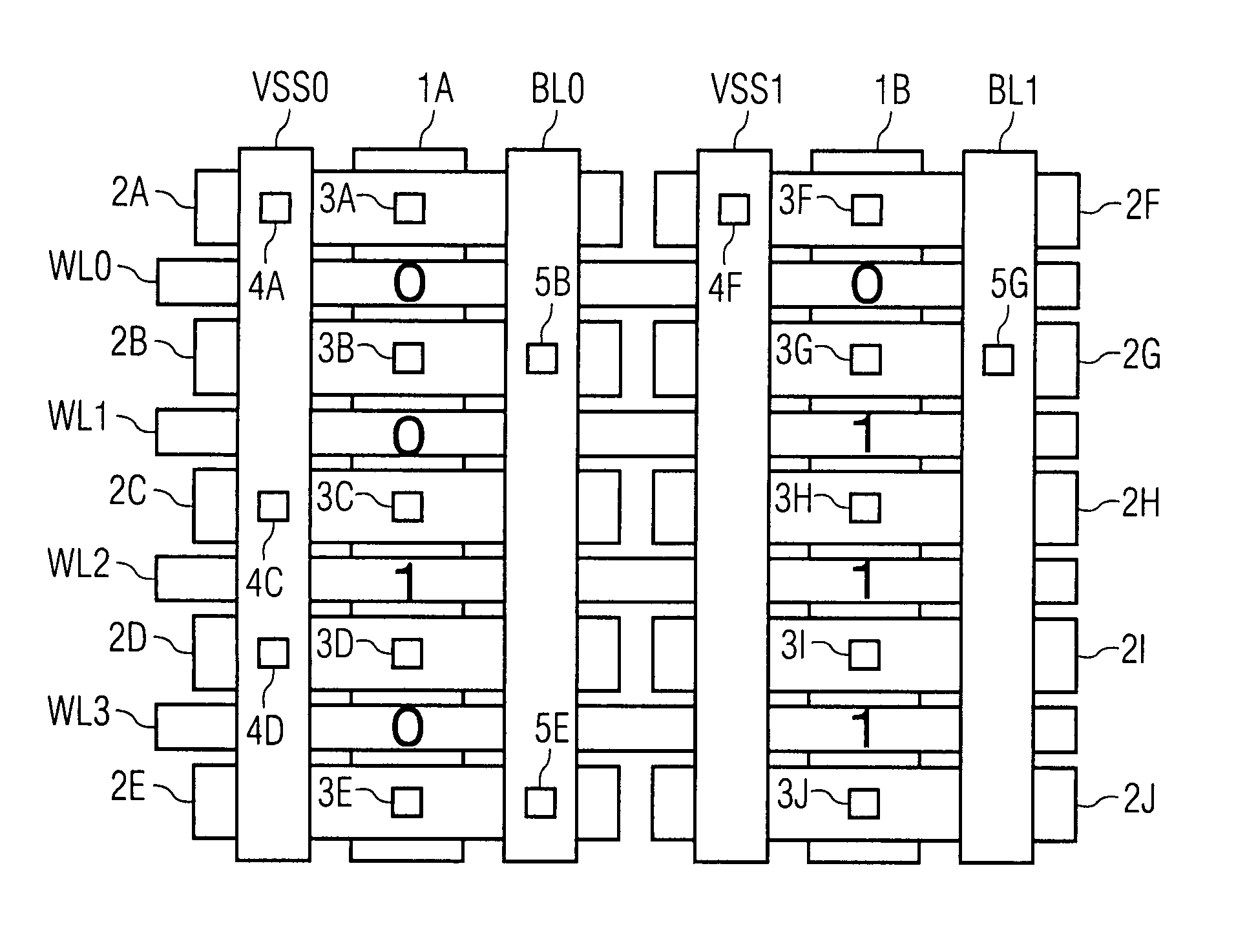
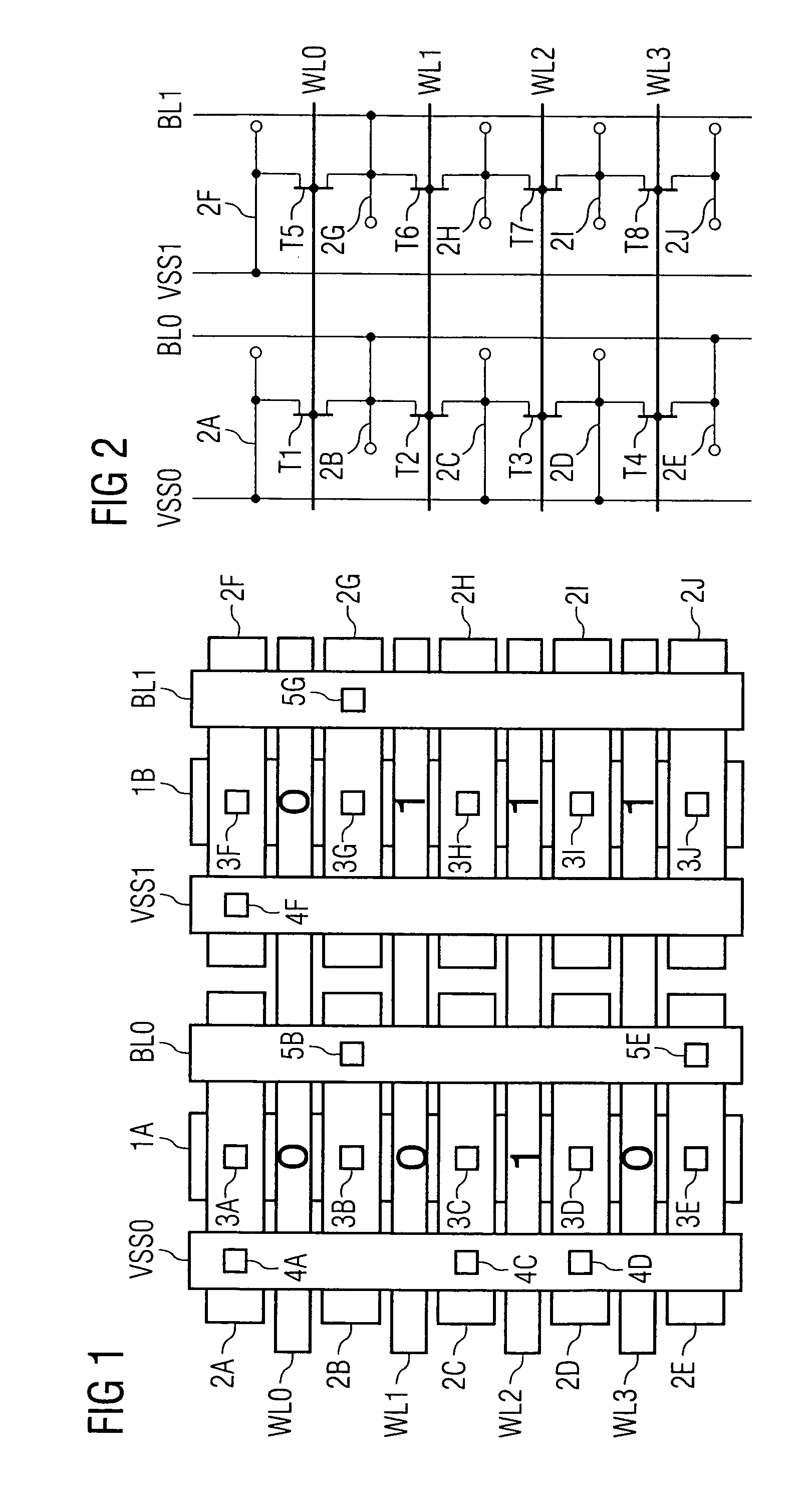
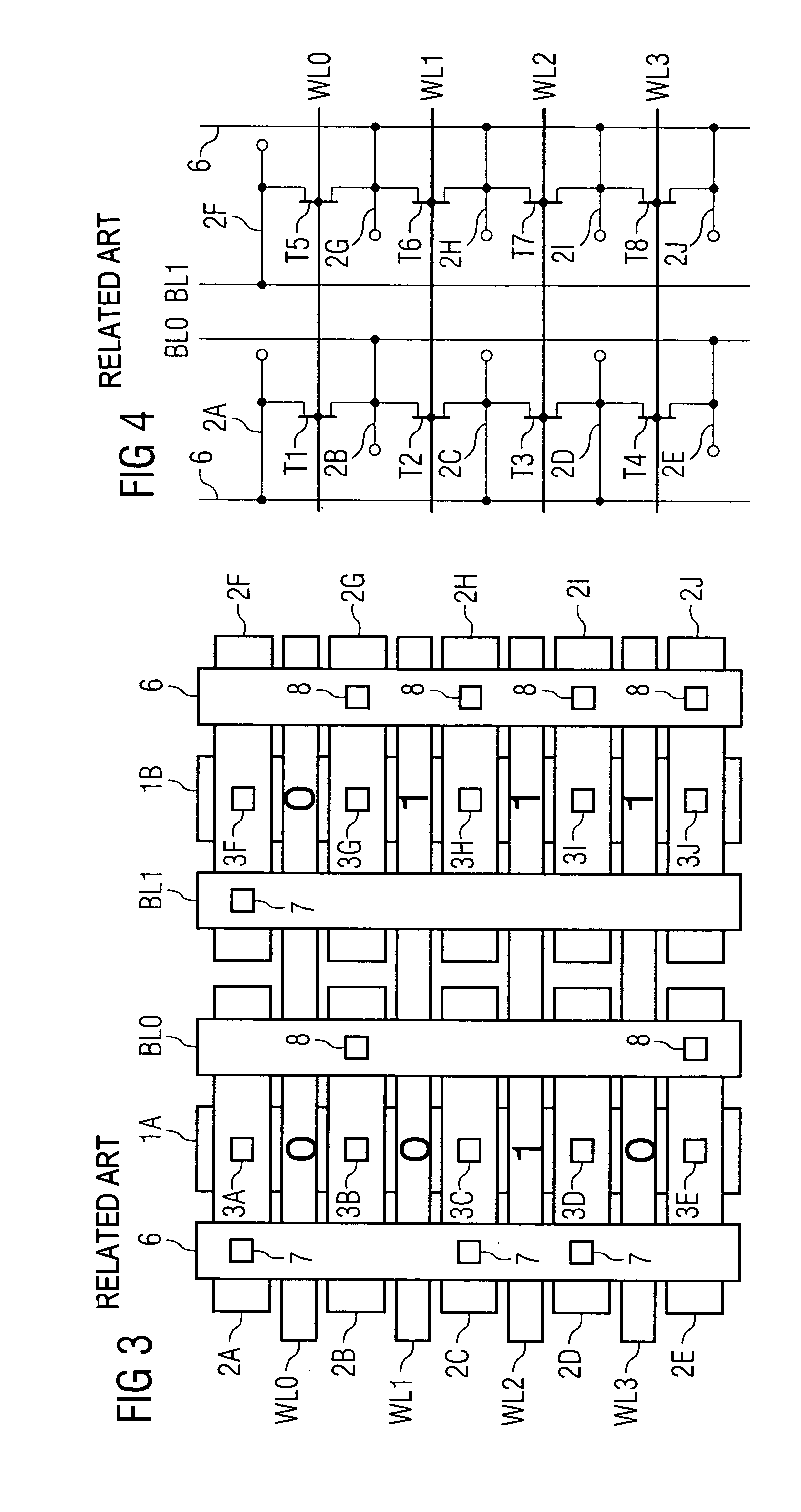
[0031]FIG. 1 shows a layout of a read-only memory or ROM embodiment of the present invention. FIG. 2 shows a corresponding circuit diagram. In FIGS. 1 and 2, similar reference labels are used to indicate similar components as those shown in FIGS. 3 and 4.

[0032]The ROM shown in FIGS. 1 and 2 comprises eight memory cells, which are arranged in two columns of four memory cells each and are formed by transistors T1–T8 as shown in the circuit diagram of FIG. 2. Naturally, ROMs used in practice contain considerably more of such memory cells, which can be arranged in more columns and rows and optionally also over one another in several layers.

[0033]The transistors T1–T8 from FIG. 2 are field-effect transistors in the embodiment shown, but in principle the use of other transistor types is also conceivable. The gate terminals of the transistors T1–T8 are connected to address lines WL0–WL3 as shown in FIG. 2; that is, two transistors are assigned one address line in each case. The source and ...


PUM


Abstract

A read-only memory arrangement and method for programming the memory arrangement are provided. The memory arrangement includes memory cells, which each have a transistor with two contacts and a control terminal, address lines, bit lines and a potential line. A combination of one of the address lines and one of the bit lines is uniquely assigned to each memory cell. The control terminal of each transistor is connected to the address line assigned to the respective memory cell. To program a memory cell into a first memory state, one of the contacts of the transistor of the memory cell is connected to the assigned bit line and the other of the contacts is connected to the potential line. To program a memory cell into a second memory state, no connections are established between the contacts of the transistor and either the assigned bit line or the potential line.

Description

CLAIM FOR PRIORITY[0001]The present application claims the benefit of German Application No. DE 10 2004 020306.7 filed on Apr. 26, 2004, which is hereby incorporated by reference.TECHNICAL FIELD[0002]The present invention relates to a method for programming a memory arrangement and a correspondingly programmed memory arrangement. In particular, the present invention relates to a method for programming a read-only memory in which the programming occurs by selective setting of metal connections (“vias”) between two metal layers.BACKGROUND[0003]Read-only memories (ROMs) are generally used for storing permanent programs or data for microprocessor systems. For example, the so-called BIOS of computer systems can be stored on such a ROM. Such ROMs are already programmed, i.e. set with data, during the production process. There are ROMs for which the programming takes place by interruption of diffusion layers (so-called “diffusion programmable ROM”). For another type of ROM, the programming...

Claims


Application Information

Patent Timeline
Patent Type & Authority Patents(United States)
IPC IPC(8): G11C17/00G11C8/00G11C17/08G11C17/12
CPCG11C17/12
Inventor MARTELLONI, YANNICKOSTERMAYR, MARTIN
Owner INFINEON TECH AG
Features
  • R&D
  • Intellectual Property
  • Life Sciences
  • Materials
  • Tech Scout
  • Unparalleled Data Quality
  • Higher Quality Content
  • 60% Fewer Hallucinations
Learn More