Continuous direct-write optical lithography

a direct-write, optical lithography technology, applied in the field of optical lithography, can solve the problems of prohibitive chip production, and high cost of reticles, and achieve the effect of reducing the cost of substrate exposure and more efficient exposur

Inactive Publication Date: 2007-01-23
CHIME BALL TECH
View PDF49 Cites 56 Cited by
  • Summary
  • Abstract
  • Description
  • Claims
  • Application Information

AI Technical Summary

Benefits of technology

[0011]In some embodiments the SLM comprises a multiplicity of area arrays. The corresponding imaging optics can be a single projection lens system, or a multiplicity of projection lens systems. In the case of the latter, the number of the area arrays is greater than the number of the projection lens systems, and the number of projection lens systems is preferably a submultiple of the number of area arrays. Furthermore, the multiplicity of area arrays can be arranged in a line, or they can be arranged in multiple lines where the placement of the arrays is staggered from one line to another. The latter may utilize more of the imaging field of the projection optics, and can also result in a more efficient exposure of the substrate—reducing the need for a serpentine motion of the projected image of the SLM across the substrate during exposure.

Problems solved by technology

The semiconductor industry uses very expensive stepper tools for lithographic processing.
Furthermore, very expensive reticles are used in this processing—the cost of the reticles is sufficient to make low volume production of chips (such as custom ASICs) prohibitively expensive.
The printed circuit board (PCB) industry has similar problems with its lithography processes.
Furthermore, the substrates used in the PCB industry undergo distortion during fabrication which limits the use of high resolution lithography processing to small area substrates and the use of steppers.

Method used


Image

  • Continuous direct-write optical lithography
  • Continuous direct-write optical lithography
  • Continuous direct-write optical lithography

Examples


Embodiment Construction

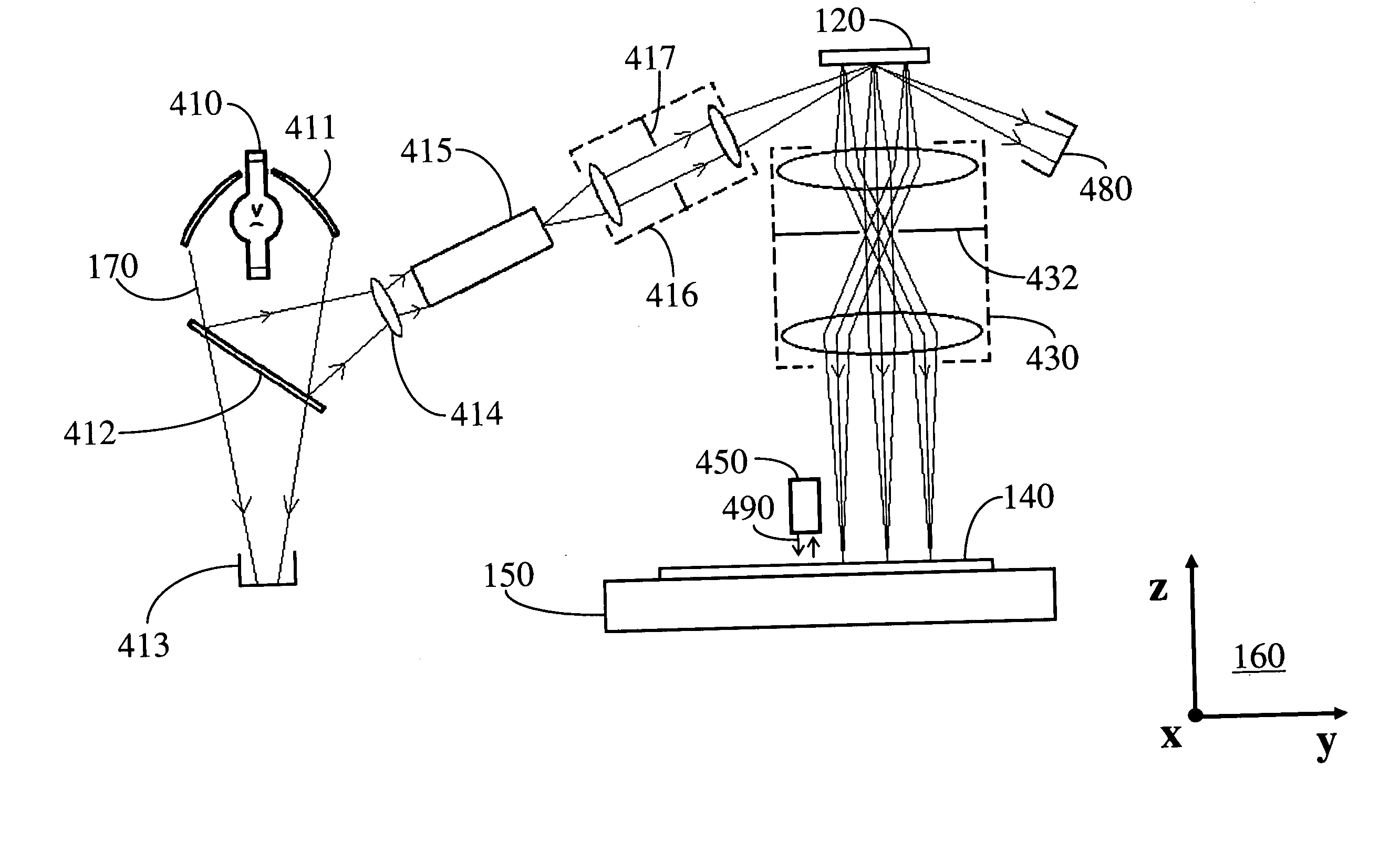
[0047]With reference to FIG. 1, optical lithography tool 100, which is an embodiment of the invention suitable for patterning a substrate 140 mounted on a movable stage 150, is shown with a light source 110, a spatial light modulator (SLM) 120 and imaging optics 130. Coordinate axes 160 are shown with the z and y axes in the plane of the figure and the x axis perpendicular to the plane of the figure. The light path through the optical lithography tool is represented by rays 170. The light source 110 continuously illuminates the SLM 120. The light source may comprise an arc lamp, continuous laser (solid state or gas), light emitting diode (LED) or other type of continuous light source that has suitable spectral properties for exposure of the substrate 140. Furthermore, a light source such as a quasi-continuous laser (a laser which is pulsed at MHz frequencies), may be suitable as a light source for this invention—a critical criteria is that the pulsing frequency be much higher than t...


PUM

PropertyMeasurementUnit
switching frequencyaaaaaaaaaa
cycle timeaaaaaaaaaa
speedaaaaaaaaaa

Abstract

An optical lithography system comprises a light source, a spatial light modulator, imaging optics and means for continuously moving a photosensitive substrate relative to the spatial light modulator. The spatial light modulator comprises at least one array of individually switchable elements. The spatial light modulator is continuously illuminated and an image of the spatial light modulator is continuously projected on the substrate; consequently, the image is constantly moving across the surface of the substrate. While the image is moving across the surface, elements of the spatial light modulator are switched such that a pixel on the surface of the substrate receives, in serial, doses of energy from multiple elements of the spatial light modulator, thus forming a latent image on the substrate surface. The imaging optics is configured to project a blurred image of the spatial light modulator on the substrate, enabling sub-pixel resolution feature edge placement.

Description

CROSS-REFERENCE TO RELATED APPLICATIONS[0001]This application claims the benefit of U.S. Provisional Application No. 60 / 406,030 filed Aug. 24, 2002, incorporated in its entirety by reference herein.BACKGROUND OF THE INVENTION[0002]1. Field of the Invention[0003]This invention relates to the field of optical lithography, and in particular to printing patterns on the following substrates: wafers; printed circuit boards; flat panel displays; masks; reticles; and plates used for the reproduction of magazines, newspapers and books.[0004]2. Description of the Related Art[0005]The semiconductor industry uses very expensive stepper tools for lithographic processing. Furthermore, very expensive reticles are used in this processing—the cost of the reticles is sufficient to make low volume production of chips (such as custom ASICs) prohibitively expensive. The semiconductor industry needs a lower cost lithography process. Furthermore, every time the lithography pattern changes, several days or...

Claims


Application Information

Patent Timeline
Patent Type & Authority Patents(United States)
IPC IPC(8): G02B26/00G03B27/42G03B27/54G03B27/72G02B27/18G03F7/20H01L21/027
CPCG03F7/70216G03F7/70275G03F7/70283G03F7/70558G03F7/70383G03F7/70466G03F7/70508G03F7/70291H01L21/0275G03F7/2024H01L21/0274
Inventor MEISBURGER, WILLIAM DANIEL
Owner CHIME BALL TECH
Why Eureka
Try Eureka