Circuit board transmitting high frequency signal
a high frequency signal and circuit board technology, applied in line-transmission details, light beam reproducing, optical beam sources, etc., can solve the problems of unnecessary radiation noise of high frequency components on the periphery, modulation may occur, and inability to accurately regenerate, etc., to achieve suppressed radiation noise
- Summary
- Abstract
- Description
- Claims
- Application Information
AI Technical Summary
Benefits of technology
Problems solved by technology
Method used
Image

Examples
first embodiment
[0028
[0029]Embodiments of the present invention will now be described in detail referring to the drawings. The same or corresponding portions in the drawings are indicated with the same characters, and descriptions thereof will not be repeated.
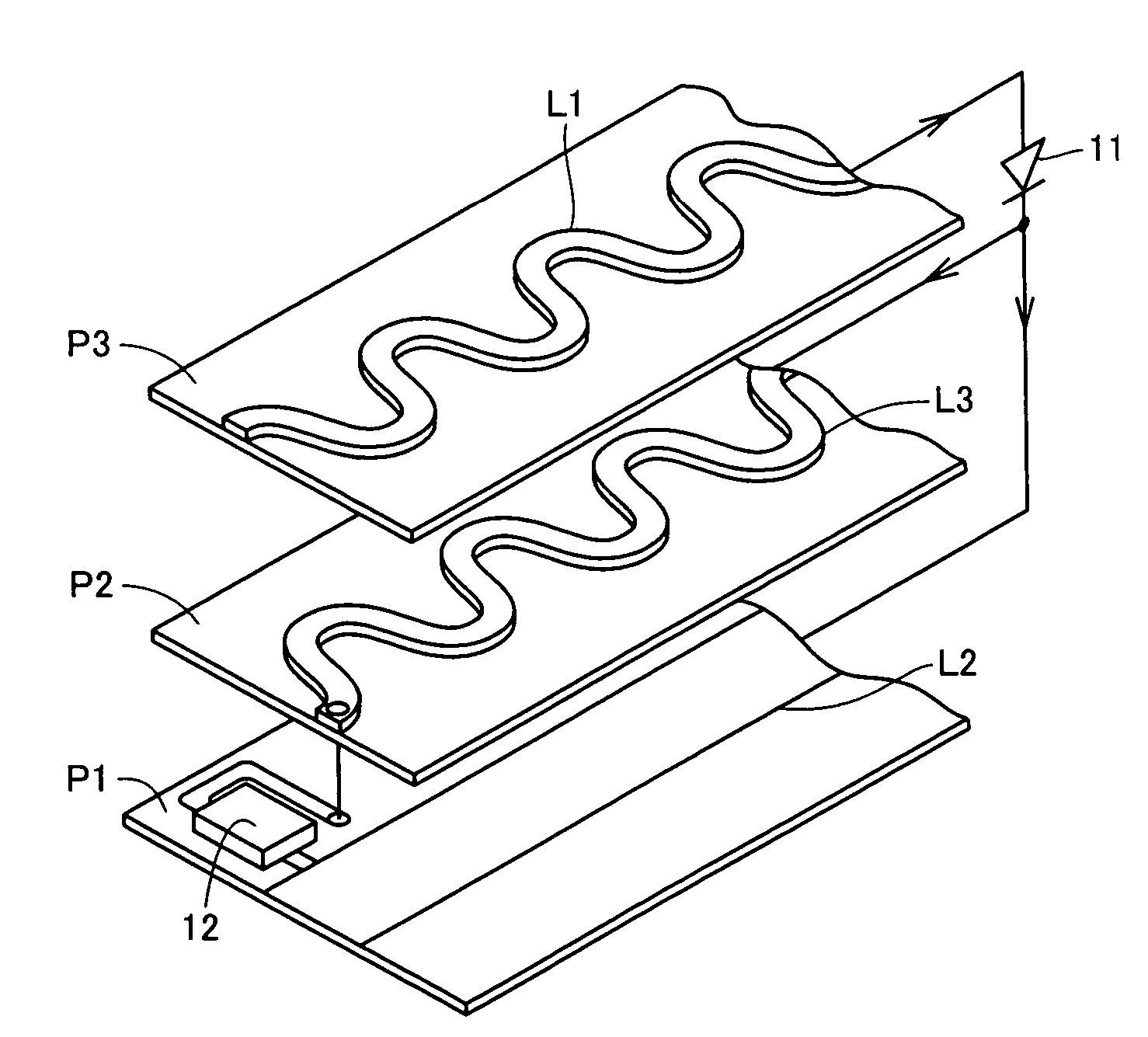
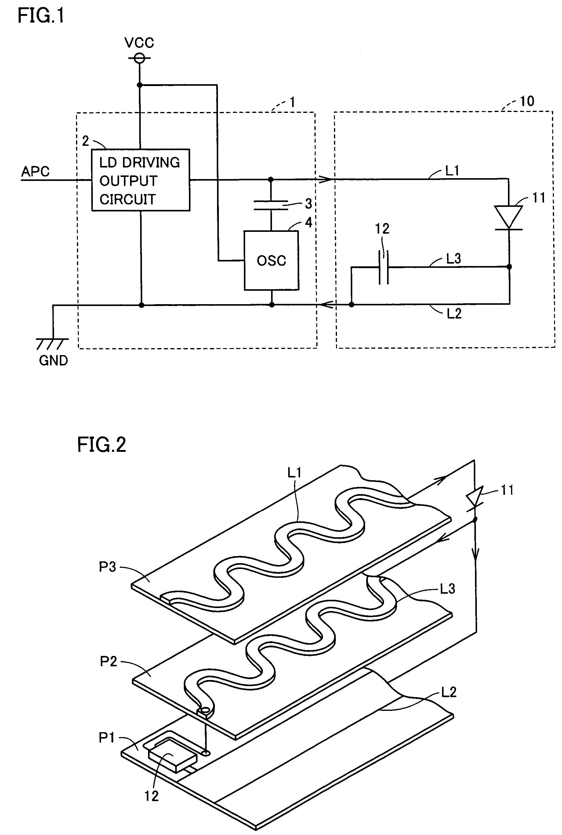
[0030]Referring to FIG. 1, a laser diode driving circuit according to a first embodiment of the present invention includes a drive unit 1 for driving a laser diode and a diode unit 10 having the laser diode.
[0031]Drive unit 1 includes an LD driving output circuit 2, an oscillator 4 (hereafter also referred to as OSC) and a capacitor 3.
[0032]Diode unit 10 includes a laser diode 11 (hereafter also simply referred to as a diode) and a capacitor 12.
[0033]LD driving output circuit 2 uses a power supply voltage VCC and a ground voltage GND as an operation voltage, and receives an input of a laser power control signal APC (hereafter also simply referred to as control signal APC) to output an LD drive signal (current) to diode unit 10. An LD drive sig...
modified example 1
[0046 of First Embodiment
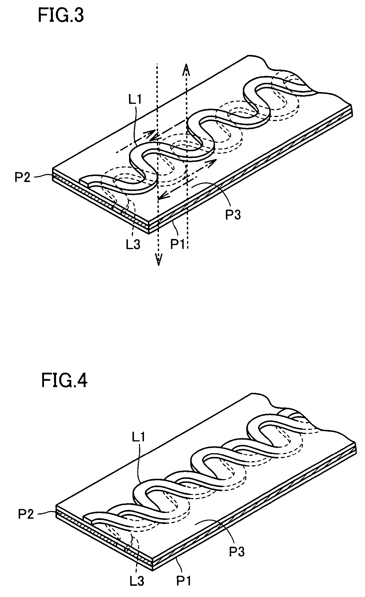
[0047]Referring to FIG. 5, in an interconnection structure of diode unit 10 according to a modified example 1 of the first embodiment of the present invention, the transmission lines formed in interconnection layers P2 and P3 are interchanged as compared with the interconnection structure shown in FIG. 2. More specifically, transmission line L3 which was formed in middle interconnection layer P2 is now formed in upper interconnection layer P3, and transmission line L1 which was formed in upper interconnection layer P3 is now formed in middle interconnection layer P2. In this construction, the output node of the diode is electrically coupled to transmission line L2 formed in lower interconnection layer P1 via contact holes CH0, CH1 and CH2. In addition, transmission line L3 is electrically coupled to capacitor 12 via contact holes CH3, CH4 and CH5.
[0048]With this interconnection structure, a circuit equivalent to diode unit 10 described in the first embodimen...
modified example 2
[0050 of First Embodiment
[0051]In each of the first embodiment and modified example 1, the construction is described in which the feedback path is divided into two paths, more specifically, into the transmission line easily passing the direct current component and the transmission line easily passing the high frequency component. In a modified example 2 of the first embodiment, a construction will be described in which the feed path is divided into two paths.
[0052]Referring to FIG. 6, as compared with the laser diode driving circuit according to the first embodiment of the present invention as shown in FIG. 1, a laser diode driving circuit according to modified example 2 of the first embodiment of the present invention is different in that, diode unit 10 is replaced with a diode unit 10a. As the other points are similar, detailed descriptions thereof will not be repeated.
[0053]Diode unit 10a includes transmission lines L4, L5 to be feed paths for transmitting the LD drive signal fro...
PUM
| Property | Measurement | Unit |
|---|---|---|
| frequency | aaaaa | aaaaa |
| frequency | aaaaa | aaaaa |
| resistance | aaaaa | aaaaa |
Abstract
Description
Claims
Application Information
 - R&D
- Intellectual Property
- Life Sciences
- Materials
- Tech Scout
- Unparalleled Data Quality
- Higher Quality Content
- 60% Fewer Hallucinations
Browse by: Latest US Patents, China's latest patents, Technical Efficacy Thesaurus, Application Domain, Technology Topic, Popular Technical Reports.
© 2025 PatSnap. All rights reserved.Legal|Privacy policy|Modern Slavery Act Transparency Statement|Sitemap|About US| Contact US: help@patsnap.com