Heterojunction semiconductor device with element isolation structure

a semiconductor device and isolation structure technology, applied in the direction of transistors, basic electric elements, radiation controlled devices, etc., can solve the problems of becoming increasingly difficult to improve the driving capability of mos transistors formed in silicon substrates, and achieve the effect of improving the element isolation characteristic of a semiconductor device and reducing the leakage current of a semiconductor elemen

Inactive Publication Date: 2007-01-30
RENESAS TECH CORP
View PDF21 Cites 8 Cited by
  • Summary
  • Abstract
  • Description
  • Claims
  • Application Information

AI Technical Summary

Benefits of technology

[0014]The present invention has for its object to provide a technique with which it is capable of reducing the leakage current of a semiconductor element and improving the element isolation characteristic of a semiconductor device.
[0016]Since the first insulating film is provided on the first semiconductor film formed on the surface of the trench, it is possible to suppress the compound semiconductor layer exposed by the trench from being directly oxidized even if the first semiconductor film is thermally oxidized to form the first insulting film. Therefore, even if an element such as germanium is contained in the compound semiconductor layer, it is possible to suppress the element from segregating in the interface between a semiconductor region including the semiconductor layer, the compound semiconductor layer and the first semiconductor film, and an insulator region including the first and second insulating films. As a result, it is capable of suppressing an increase in the interface state density in the interface between the semiconductor region and the insulator region, thereby reducing the leakage current of the semiconductor element provided in the element forming region. It is also capable of suppressing an increase in the fixed charge in the first insulating film, thereby improving the element isolation characteristic in the semiconductor device.

Problems solved by technology

Recently, it is becoming increasingly difficult to improve the driving capability of a MOS transistor formed in a silicon substrate, which is the most important for achieving high operating speed of a CMOS device.

Method used


Image

  • Heterojunction semiconductor device with element isolation structure
  • Heterojunction semiconductor device with element isolation structure
  • Heterojunction semiconductor device with element isolation structure

Examples


first preferred embodiment

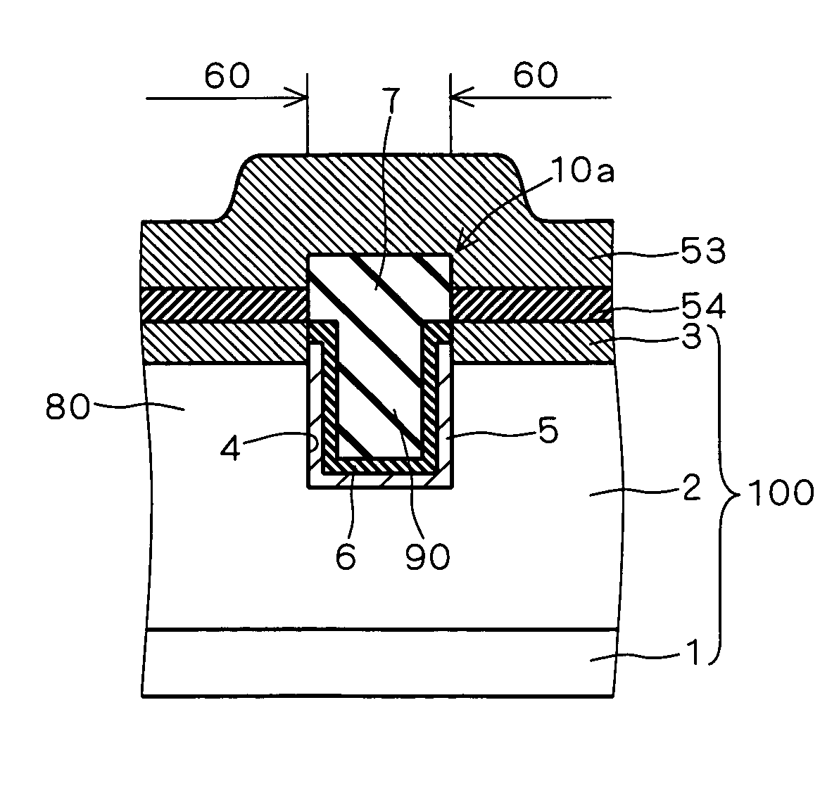
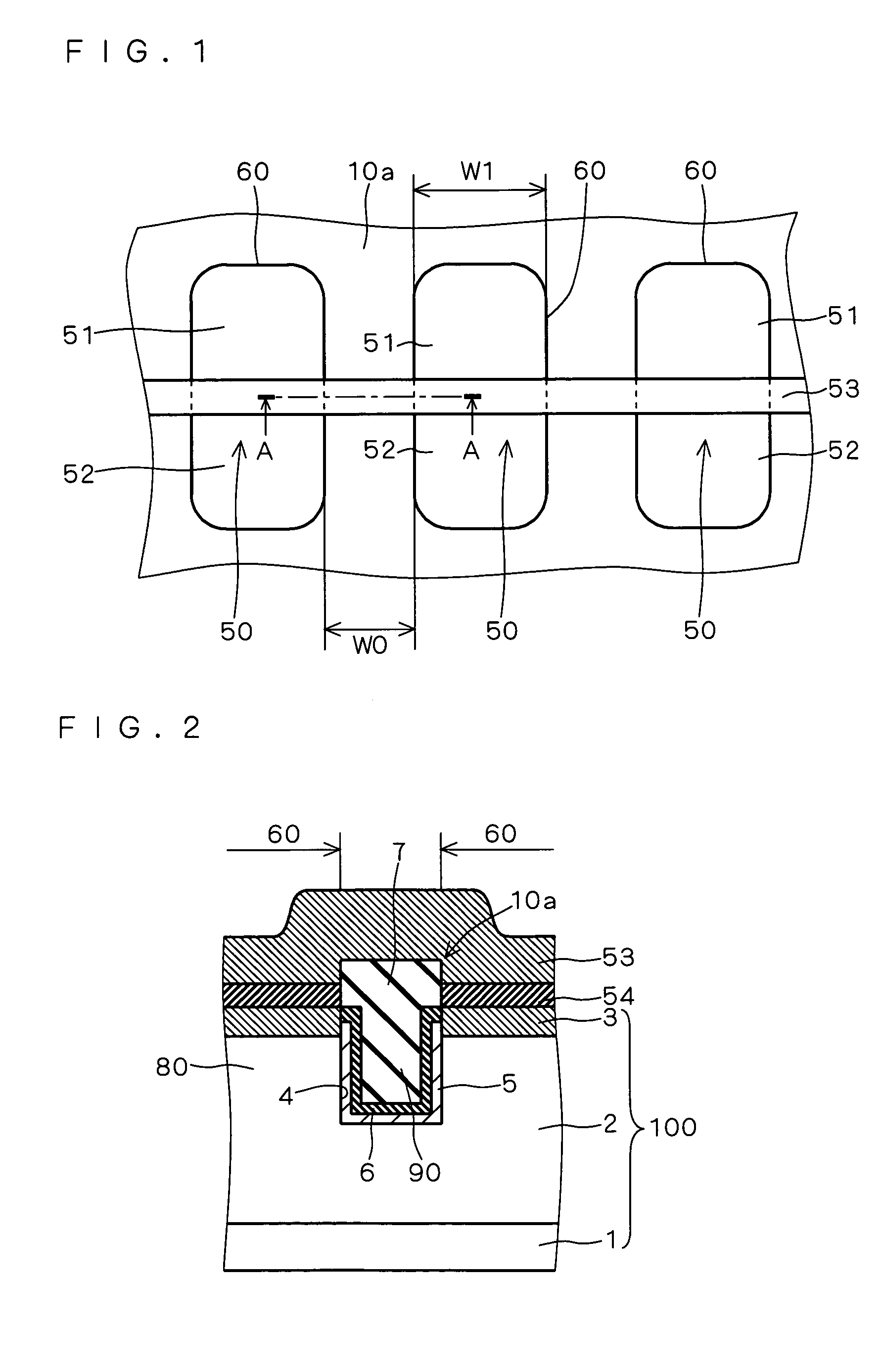
[0030]FIG. 1 is a plan view showing the structure of a semiconductor device according to a first preferred embodiment of the present invention. FIG. 2 is a sectional view taken along the line A—A as indicated by the arrows in FIG. 1. As shown in FIGS. 1 and 2, the semiconductor device of the first preferred embodiment has a semiconductor substrate 100. The semiconductor substrate 100 has a silicon substrate 1, a compound semiconductor layer 2, and a semiconductor layer 3. The compound semiconductor layer 2 is a SiGe layer, for example. The semiconductor layer 3 is a Si layer, for example. The silicon substrate 1, the compound semiconductor layer 2 and the semiconductor layer 3 are laminated in this order, and the compound semiconductor layer 2 and the semiconductor layer 3 form heterojunction. As a result, the semiconductor layer 3 becomes a strained Si layer.

[0031]An element isolation structure 10a is formed in the semiconductor substrate 100, and a plurality of element forming reg...

second preferred embodiment

[0054]FIG. 9 is a sectional view showing the structure of a semiconductor device according to a second preferred embodiment of the present invention. FIG. 10 is a sectional view showing in enlarged dimension the area B in FIG. 9. The semiconductor device of the second preferred embodiment differs from the semiconductor device of the first preferred embodiment in that an element isolation structure 10b is provided instead of the element isolation structure 10a. The element isolation structure 10b has a semiconductor film 5 and an insulating film 6 that are of different shapes than in the element isolation structure 10a. Note that FIG. 9 is a sectional view taken at a location corresponding to the line A—A as indicated by the arrows in FIG. 1.

[0055]As shown in FIGS. 9 and 10, the semiconductor film 5 provided on the surface of a trench 4 is in contact with the entire region of the inner surface of a compound semiconductor device 2 that is exposed by a trench 4, and with the entire reg...

third preferred embodiment

[0066]FIG. 14 is a plan view showing the structure of a semiconductor device according to a third preferred embodiment of the present invention. FIG. 15 is a sectional view taken along the line C—C as indicated by the arrows in FIG. 14. FIG. 16 is sectional view showing in enlarged dimension the area D in FIG. 15. In FIG. 14, a semiconductor film 35 is omitted to avoid the complexity of the drawing. A semiconductor device of the third preferred embodiment is basically the same as the semiconductor device of the first preferred embodiment, except that an element isolation structure 10c is provided instead of the element isolation structure 10a, and that the semiconductor film 35 is added. The element isolation structure 10c has a semiconductor film 5 and an insulating film 6 that are of different shapes than in the element isolation structure 10a of the first preferred embodiment.

[0067]Referring to FIGS. 14 to 16, a semiconductor film 5 provided on the surface of a trench 4 is in con...


PUM


Abstract

A technique enabling to improve element isolation characteristic of a semiconductor device is provided. An element isolation structure is provided in a semiconductor substrate in which a silicon layer, a compound semiconductor layer and a semiconductor layer are laminated in this order. The element isolation structure is composed of a trench, a semiconductor film, and first and second insulating films. The trench extends through the semiconductor layer and extends to the inside of the compound semiconductor layer. The semiconductor film is provided on the surface of the trench, and the first insulating film is provided on the semiconductor film. The second insulting film is provided on the first insulating film and fills the trench. Since the semiconductor film is interposed between the compound semiconductor film which is exposed by the trench and the first insulating film, there is no possibility that the compound semiconductor layer is directly thermally oxidized even if the semiconductor film is thermally oxidized to form the first insulating film.

Description

BACKGROUND OF THE INVENTION[0001]1. Field of the Invention[0002]The present invention relates to a semiconductor device provided with an element isolation structure.[0003]2. Description of the Background Art[0004]Recently, it is becoming increasingly difficult to improve the driving capability of a MOS transistor formed in a silicon substrate, which is the most important for achieving high operating speed of a CMOS device. As a technique for overcoming this, there has been proposed a method for forming a MOS transistor by utilizing heterojunction to be formed by silicon (Si) and silicon germanium (SiGe).[0005]Based on the document of Kern (Kim) Rim et al., “Fabrication and Analysis of Deep Submicron Strained-Si N-MOSFET's,” IEEE Transactions on Electron Devices, 2000, Vol. 47, No. 7, pp. 1406–1415 (hereinafter referred to as a “document I”), a silicon germanium layer (hereinafter referred to as a “SiGe layer”) after being subjected to lattice relaxation is formed on a silicon substr...

Claims


Application Information

Patent Timeline
Patent Type & Authority Patents(United States)
IPC IPC(8): H01L31/072H01L23/48H01L31/0328H01L31/0336H01L31/109H01L21/76H01L21/336H01L21/762H01L21/8234H01L29/78
CPCH01L21/76224H01L21/823481H01L2924/0002H01L2924/00H01L21/762H01L21/76
Inventor SUGIHARA, KOHEIOTA, KAZUNOBUODA, HIDEKAZUHAYASHI, TAKAHASHI
Owner RENESAS TECH CORP
Why Eureka
Try Eureka