
High-frequency wiring structure and method for producing the same

a high-frequency wiring and high-frequency current technology, applied in the direction of waveguides, conductive pattern formation, waveguide type devices, etc., can solve the problems of high loss, circuit board undetectedly showing higher loss, limited region through which high-frequency current passes, etc., to reduce the loss of high-frequency current and large cross-sectional area

Inactive Publication Date: 2007-02-06
ALPS ALPINE CO LTD
View PDF10 Cites 3 Cited by
  • Summary
  • Abstract
  • Description
  • Claims
  • Application Information

AI Technical Summary

Benefits of technology

[0008]An object of the present invention is to solve the above problems and provide a high-frequency wiring structure that can prevent loss of high-frequency current due to partial concentration and reduce loss of high-frequency current with a transmission conductor having a larger cross-sectional area, and a method for producing the high-frequency wiring structure.
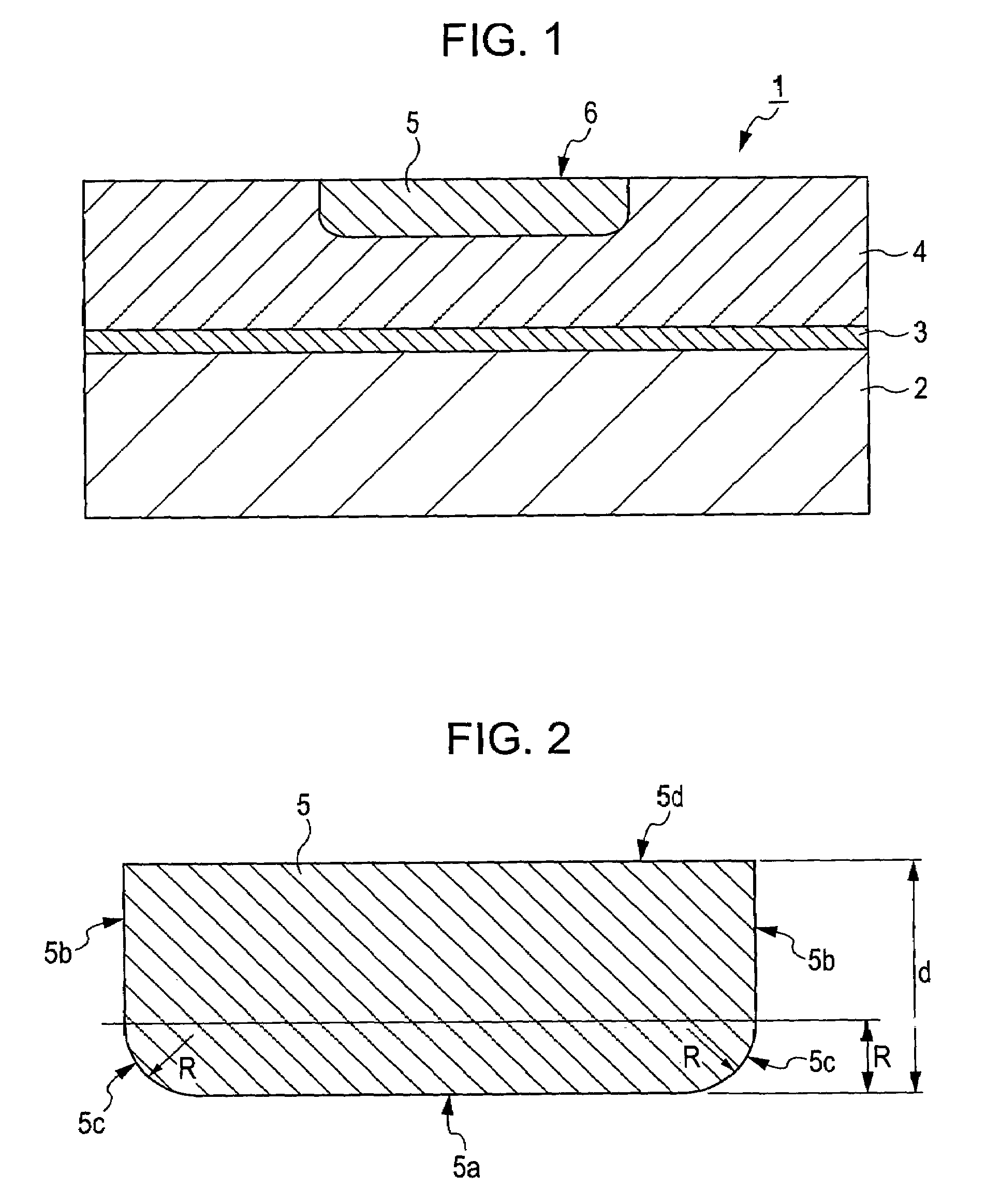
[0010]According to the above structure, the curved parts, having a radius of curvature within the above range, can relieve the concentration of high-frequency current to reduce high-frequency loss. Moreover, the transmission conductor, having the flat sides in addition to the flat bottom, can attain a larger cross-sectional area than a transmission conductor in conventional circuit wiring to reduce the high-frequency loss. Furthermore, the curved parts and the flat sides are continuously joined to relieve the concentration of high-frequency current, thus reducing the loss.
[0011]In the above high-frequency wiring structure according to the present invention, the curved parts preferably have a radius of curvature within the range of 10% to 40% of the thickness of the transmission conductor. Such a structure can further relieve the concentration of high-frequency current, thus attaining a smaller loss.
[0016]The high-frequency wiring structure according to the present invention can prevent loss of high-frequency current due to partial concentration and reduce loss of high-frequency current with a transmission conductor having a larger cross-sectional area.

Problems solved by technology

For the circuit board disclosed in Patent Document 1, however, the region through which high-frequency current passes is limited to the curved parts of the transmission conductor.
As a result, the cross-sectional area of the transmission conductor is small relative to the designed line width; this circuit board undesirably exhibits higher loss.
As a result, unfortunately, high-frequency current readily concentrates on the sharp edges, leading to higher loss.

Method used


Image

  • High-frequency wiring structure and method for producing the same
  • High-frequency wiring structure and method for producing the same
  • High-frequency wiring structure and method for producing the same

Examples


first embodiment

[First Embodiment]

[0023]A first embodiment of the present invention will now be described with reference to the drawings. FIG. 1 is a schematic sectional view of a high-frequency wiring structure according to this embodiment. FIG. 2 is a schematic sectional view of the main part of the high-frequency wiring structure. Referring to FIG. 1, a high-frequency wiring structure 1 according to this embodiment includes a microstrip line 6 having an insulating substrate 2, a ground conductor 3 formed on the insulating substrate 2, a dielectric 4 disposed on the ground conductor 3, and a transmission conductor 5 that is at least partially disposed in the dielectric 4.

[0024]The insulating substrate 2 used may be any substrate that can support the ground conductor 3 and the dielectric 4, for example a glass epoxy substrate or an alumina substrate. The insulating substrate 2, which is not an essential component, may be omitted if the dielectric 4 has relatively high strength.

[0025]The ground con...

second embodiment

[Second Embodiment]

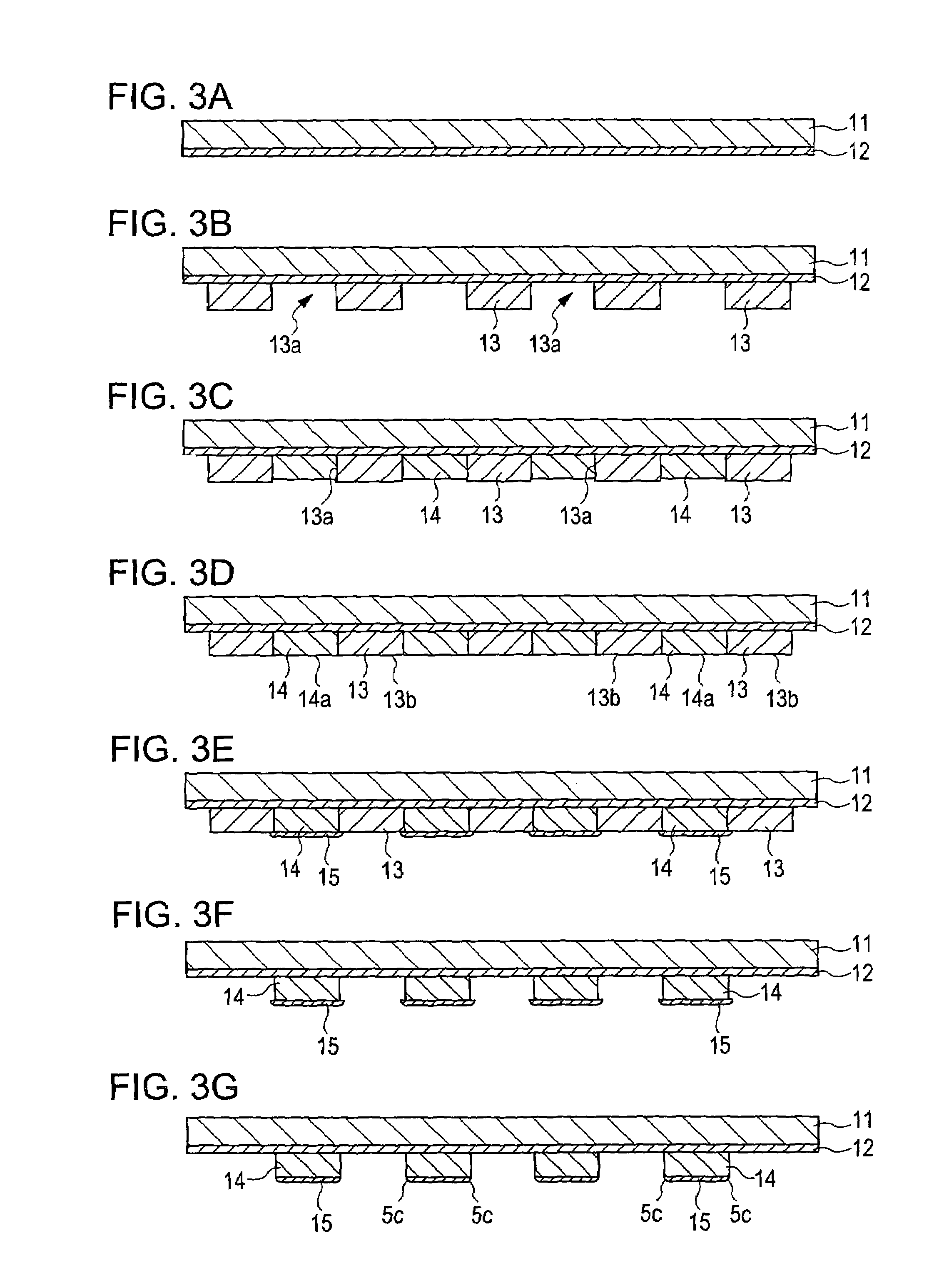
[0035]A method for producing a high-frequency wiring structure according to a second embodiment of the present invention will now be described. FIGS. 3A to 3G and 4A to 4D illustrate the steps of the method for producing a high-frequency wiring structure according to this embodiment. The method for producing a high-frequency wiring structure according to this embodiment mainly includes the steps of forming a mask resist layer on a substrate, forming first patterned conductors, forming second patterned conductors, processing the second patterned conductors to form curved surfaces, embedding the first and second patterned conductors into a dielectric, and removing the substrate.

[0036]In the step of forming the mask resist layer on the substrate, a conductive seed layer is formed on the substrate, and the mask resist layer is formed on the conductive seed layer. Conductor pattern portions are opened in the mask resist layer. Referring to FIG. 3A, a conductive seed la...

third embodiment

[Third Embodiment]

[0051]A method for producing a high-frequency wiring structure according to a third embodiment of the present invention will now be described. FIGS. 5A to 5E illustrate the steps of the method for producing a high-frequency wiring structure according to this embodiment. The method for producing a high-frequency wiring structure according to this embodiment mainly includes the steps of forming a mask resist layer on a substrate, forming first patterned conductors, forming second patterned conductors, removing the mask resist layer together with parts of the second patterned conductors by a lift-off process, embedding the first and second patterned conductors into a dielectric, and removing the substrate.

[0052]Some steps of the method for producing a high-frequency wiring structure according to this embodiment are the same as in the method according to the second embodiment described above: the step of forming the mask resist layer, the step of embedding the first an...


PUM


Abstract

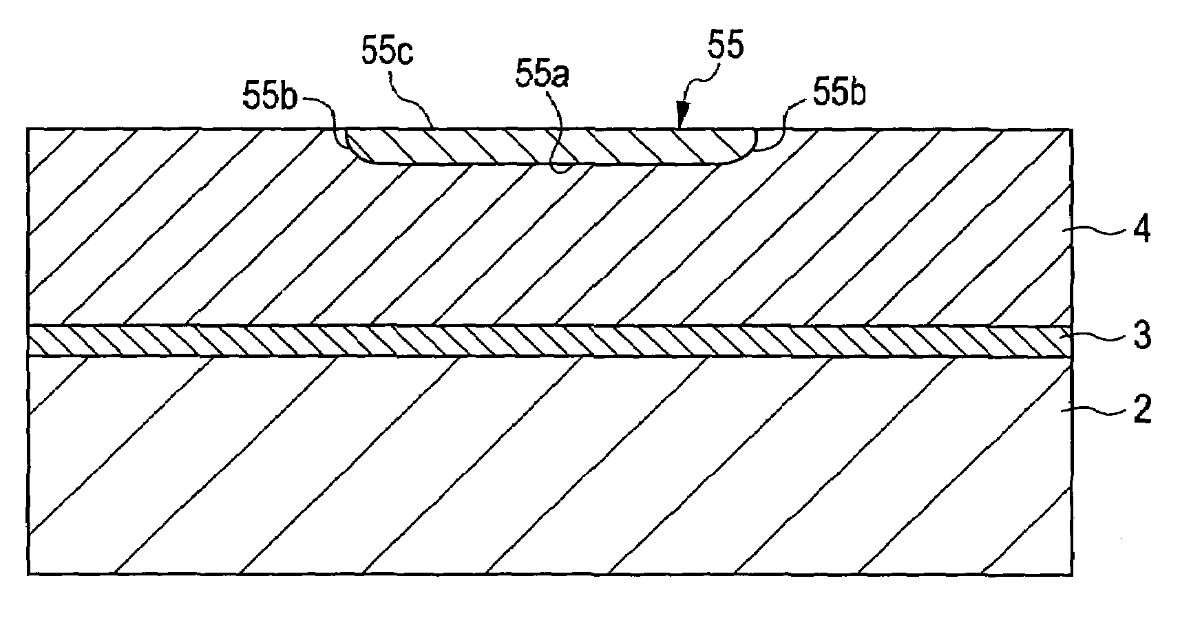
A high-frequency wiring structure includes a microstrip line having a ground conductor, a dielectric disposed on the ground conductor, and a transmission conductor that is at least partially disposed in the dielectric. The transmission conductor is defined by a flat bottom parallel to the ground conductor, a pair of flat sides that are perpendicular to the ground conductor and are positioned on both sides of the flat bottom in the wiring width direction, and curved parts that continuously join the flat bottom and the pair of flat sides. The curved parts have a radius of curvature within the range of 5% to 50% of the thickness of the transmission conductor.

Description

BACKGROUND OF THE INVENTION[0001]1. Field of the Invention[0002]The present invention relates to high-frequency wiring structures and methods for producing the high-frequency wiring structures and, particularly, to a high-frequency wiring structure capable of reducing loss and a method for producing the high-frequency wiring structure.[0003]2. Description of the Related Art[0004]Increasing application of high frequencies, including microwaves and millimeter waves, for consumer products has recently been expanding the field of radio communications, such as mobile radio communications, satellite communications, and vehicle collision avoidance systems. Accordingly, higher frequencies are used for data communications, and signals with higher frequencies are processed in transmitters and receivers.[0005]General transmitters and receivers include a printed circuit board or ceramic board, a dielectric layer formed thereon, and a fine circuit pattern (wiring pattern) formed thereon. ICs and...

Claims


Application Information

Patent Timeline
Patent Type & Authority Patents(United States)
IPC IPC(8): H01L21/44H01L21/469H01L21/50H01L21/48H01L21/68H01L23/053H01L23/12H01L23/52H01P3/08H01P11/00H05K1/02H05K3/02H05K3/04H05K3/10H05K3/18H05K3/20H05K3/22
CPCH01L21/6835H01P3/081H01P3/088H05K1/0242H05K3/205H01P11/003H01L2221/68363H05K2201/098H05K3/048H05K3/108
Inventor SASAKI, YORIHIKO
Owner ALPS ALPINE CO LTD
Learn More