Semiconductor device manufacture method and etching system

a semiconductor device and manufacturing method technology, applied in semiconductor devices, semiconductor/solid-state device testing/measurement, instruments, etc., can solve the problems of changing the pattern width, reducing the number of reticles, so as to achieve the target pattern width stably through trimming

Active Publication Date: 2007-02-06
FUJITSU SEMICON LTD
View PDF4 Cites 2 Cited by
  • Summary
  • Abstract
  • Description
  • Claims
  • Application Information

AI Technical Summary

Benefits of technology

[0013]An object of this invention is to provide a semiconductor device manufacture method capable of stably realizing a target pattern width through trimming using plasma etching.
[0014]Another object of this invention is to provide a semiconductor device manufacture method capable of stably realizing a target pattern width through trimming using plasma etching, independently from the pattern density.

Problems solved by technology

Also in this case, the problem is the density difference between final resist pattern widths.
However, in the etching process, there exists a long term variation that etching products deposited on the wall of an etching system are released in a later etching process, and this long term variation changes the pattern widths due to a density difference.
If this variation is to be dealt with reticle correction, the number of reticles becomes enormous, which is not practical.

Method used


Image

  • Semiconductor device manufacture method and etching system
  • Semiconductor device manufacture method and etching system
  • Semiconductor device manufacture method and etching system

Examples


Embodiment Construction

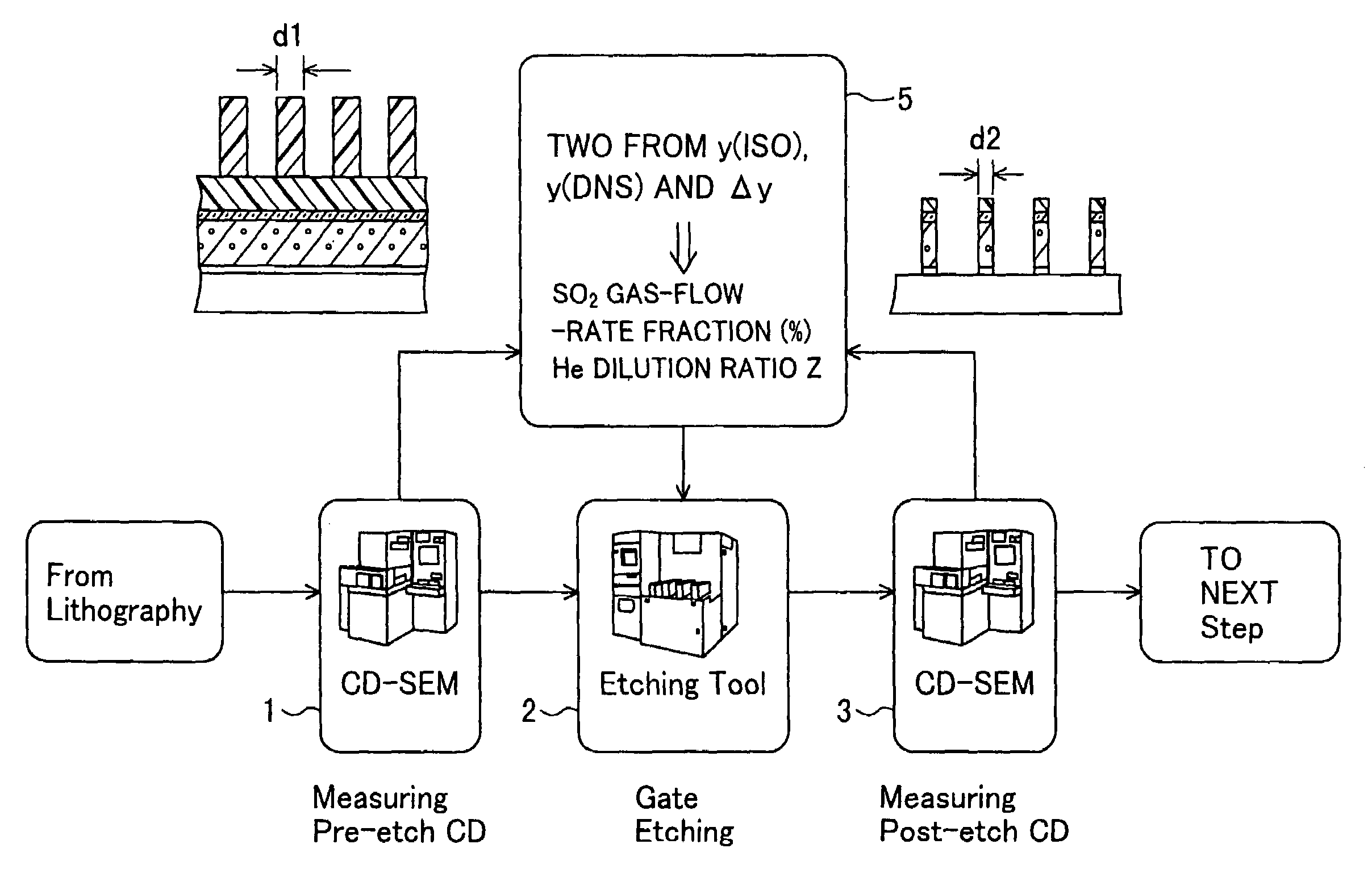
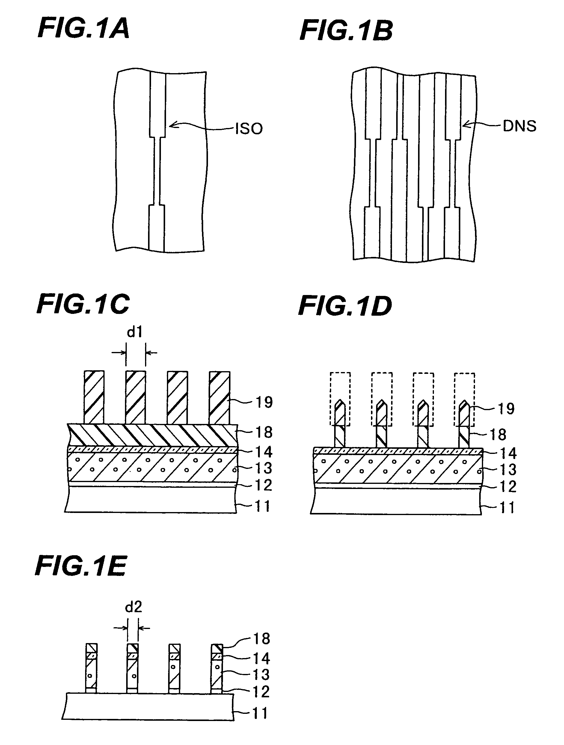
[0042]The present inventor has studied a method of forming a gate electrode having a gate length narrower than a scale limit of photolithography. If a resist pattern is trimmed by plasma etching, an etching rate changes with whether the density of patterns is dense or coarse, and gate lengths in a wafer become irregular.

[0043]If a resist pattern is formed on a BARC layer, the BARC layer is etched by using the resist pattern as a mask. Etching the resist pattern while the BARC layer is etched can be utilized for trimming. However, if the resist pattern is etched by plasma etching, the etching rate changes with the pattern density and resultant pattern widths are often irregular due to the influence of the pattern density.

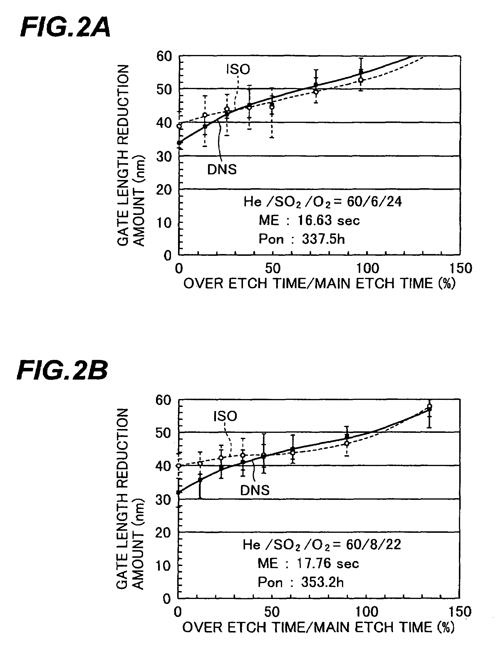
[0044]As a method of correcting a difference among etching amounts to be caused by the pattern density, it is known that a mixed gas of a plurality of gasses having different etching characteristics is used. The present inventor has checked how a pattern width change...


PUM

PropertyMeasurementUnit
gate lengthaaaaaaaaaa
thicknessaaaaaaaaaa
thickaaaaaaaaaa

Abstract

A semiconductor device manufacture method includes the steps of forming a resist layer above a work target layer; exposing and developing the resist layer to form resist patterns including isolated pattern and dense patterns; monitoring widths of isolated and dense pattern of the resist patterns to determine trimming amounts of linewidths to be reduced; determining etching conditions for realizing the trimming amounts of both the isolated and dense patterns, the etching conditions using mixed gas of a gas having a function of mainly enhancing etching and a gas having a function of mainly suppressing etching; trimming the resist pattern under said determined etching conditions; and etching the work target layer by using said trimmed resist patterns. A desired pattern width an be realized stably by trimming using plasma etching.

Description

CROSS REFERENCE TO RELATED APPLICATION[0001]This application is based on and claims priority of Japanese Patent Applications No. 2003-194380 filed on Jul. 9, 2003 and No. 2004-158165 filed on May 27, 2004, the entire contents of which are incorporated herein by reference.BACKGROUND OF THE INVENTION[0002]A) Field of the Invention[0003]The present invention relates to a semiconductor device manufacture method and an etching system, and more particularly to a semiconductor device manufacture method including a process of trimming fine resist pattern such as a pattern used for patterning gate electrodes, and an etching system suitable for embodying this method.[0004]B) Description of the Related Art[0005]The operation speed of a MOS transistor is greatly influenced by a gate length. The shorter the gate length, the high speed operation of the transistor becomes easier. As the gate length is shortened by scaling, the gate length of 100 nm or shorter has been adopted. Such a short gate le...

Claims


Application Information

Patent Timeline
Patent Type & Authority Patents(United States)
IPC IPC(8): H01L21/302H01L21/461G03F7/00H01L21/3065H01L21/00H01L21/027H01L21/28H01L21/311H01L21/3213H01L21/66
CPCH01L22/20H01L21/32139H01L21/31138H01L21/28123
Inventor GOTO, TAKESHITAJIMA, MITSUGUYAMAZAKI, TAKAYUKIKATO, TAKAYA
Owner FUJITSU SEMICON LTD
Why Eureka
Try Eureka