High speed chip-to-chip communication links

a communication link and high-speed technology, applied in the direction of logic circuit coupling/interface arrangement, digital transmission, pulse technique, etc., can solve the problems of too limited to approximately 10 gbps per channel, limitations in certain applications,

Active Publication Date: 2007-02-13
NORTHROP GRUMMAN SYST CORP
View PDF4 Cites 5 Cited by
  • Summary
  • Abstract
  • Description
  • Claims
  • Application Information

AI Technical Summary

Benefits of technology

[0010]According to the present invention, a very low voltage swing is used to achieve very high data rates (up to 4 Gbps double data rate) at very low power consumption. A differential signaling approach is used for noise rejection, and a constant current approach also is used to minimize switching noise.
[0012]According to an embodiment of the present invention, the differential swing and common mode are decreased so as to effectively increase the data speed and lower the power usage of integrated circuit chip I / O cells. To accomplish this, according to one exemplary embodiment of the invention novel designs of amplifier, inverter, ESD (electrostatic discharge) protection, current mirror, and current driver components are provided to achieve the desired data transfer speed and power consumption goals.
[0013]In particular, according to one aspect of the invention, an input / output interface circuit for transferring data between integrated circuit chips is provided, which includes a driver circuit including an inverter stage and a constant current driving stage, that receives an input data signal and develops a differential voltage signal corresponding thereto, a receiver circuit that receives the differential voltage signal from the driver circuit, including a differential in / differential out amplifier stage that receives the differential voltage signal and outputs an amplified differential signal, a differential in / single-ended out amplifier stage that receives said amplified differential signal and outputs a voltage swing signal, and an inverter stage for increasing drive strength of said voltage swing signal for transfer into a chip core.

Problems solved by technology

Discrete channel fiber-optical connections are being incorporated on top of the metal interconnections, but they too are limited to approximately 10 Gbps per channel.
Even with all these benefits, there are some limitations in certain applications, including support of multipoint bus configurations, operation from still lower power rail voltage, and extended receiver common-mode range.

Method used


Image

  • High speed chip-to-chip communication links
  • High speed chip-to-chip communication links
  • High speed chip-to-chip communication links

Examples


Embodiment Construction

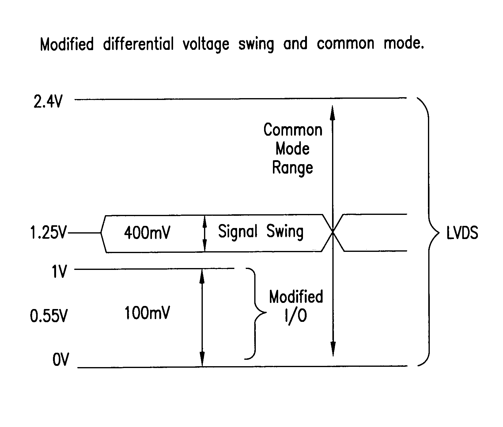
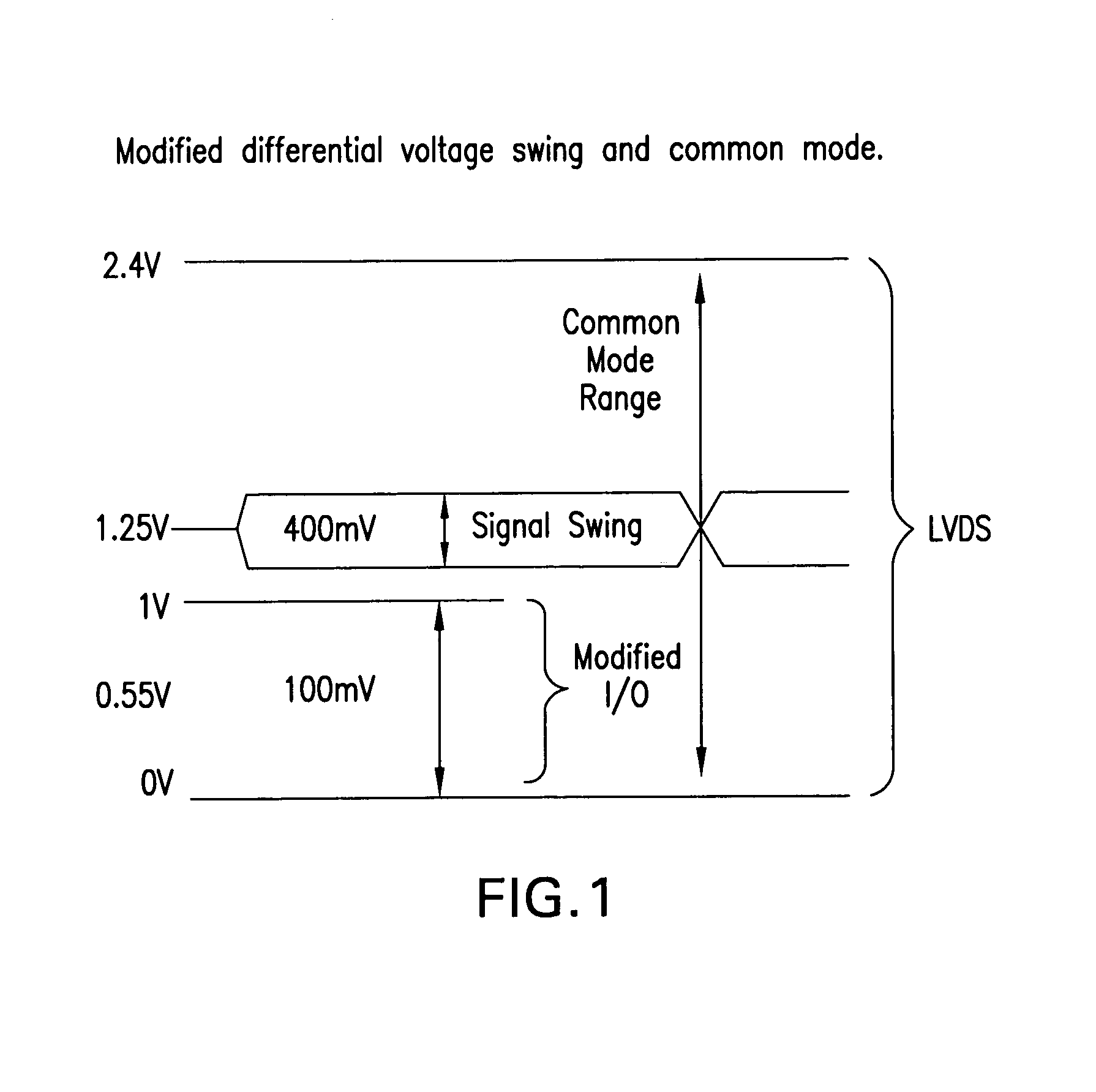
[0019]FIG. 1 illustrates the difference between a conventional LVDS signaling standard and the modified design according to one preferred embodiment of the invention. As shown, according to a conventional LVDS standard, a common mode voltage range of 2.4 V, and a differential signal swing of 400 mV at 1.25 V are used. According to one embodiment of the present invention, a modified common mode range of 1 V is used, along with a differential signal swing of 100 mV at 0.55 V. In order to realize the use of such modified levels, new designs of circuit components for both a receiver and driver circuit are provided.

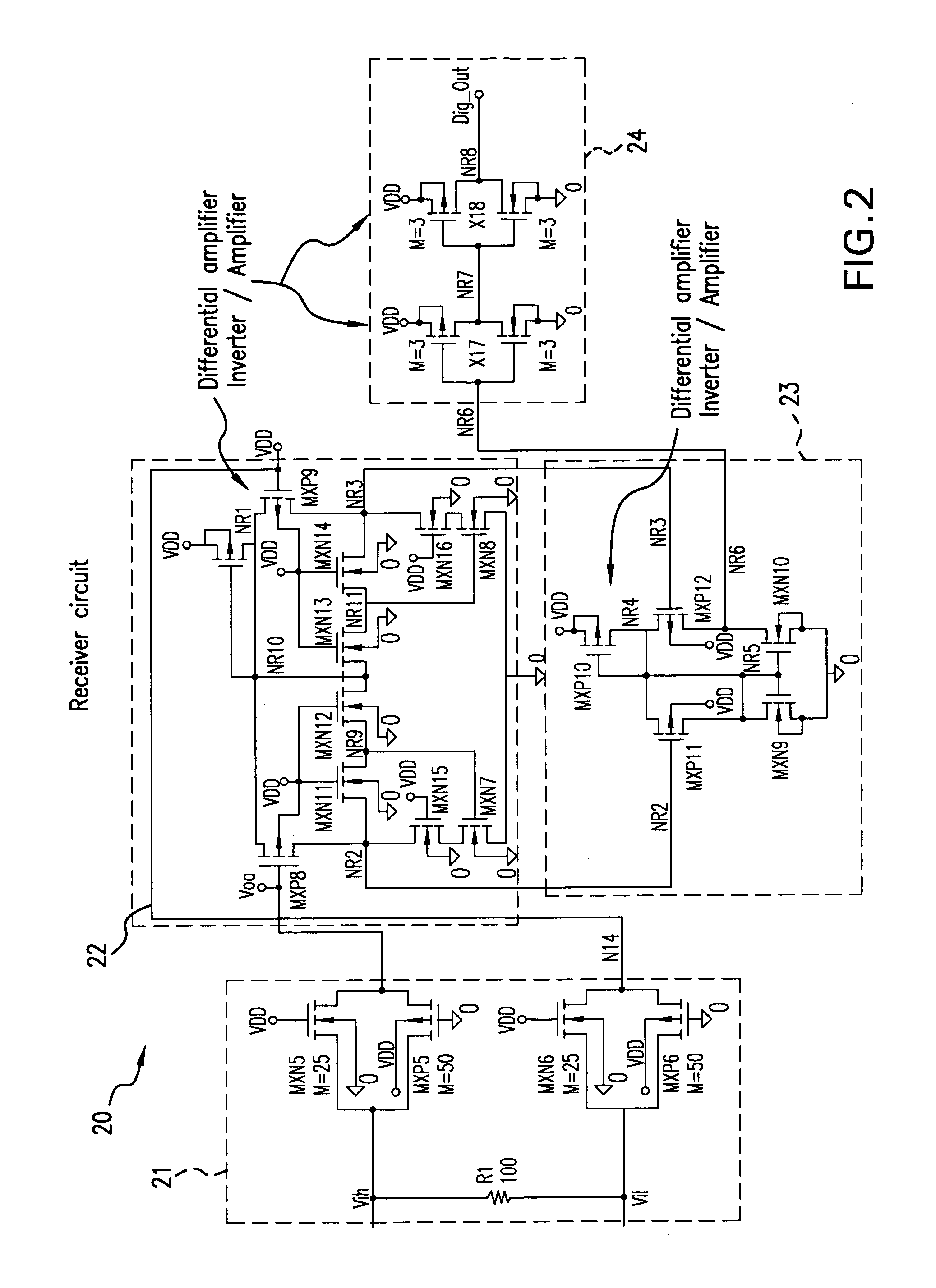
[0020]Referring to FIG. 2, one preferred embodiment of a receiver circuit 20 according to the present invention is disclosed. A first stage of the receiver circuit is an ESD protection stage 21, including a pair of modified transmission gates, a first of which receives a high differential voltage input Vih, and a second of which receives a low differential voltage input Vil, a...


PUM


Abstract

A very low voltage swing is used to achieve very high data rates (up to 4 Gbps double data rate) at very low power consumption. A differential signaling approach is used for noise rejection, and a constant current approach also is used to minimize switching noise.

Description

GOVERNMENT LICENSE RIGHTS[0001]The United States Government may have certain rights in some aspects of the invention claimed herein, as the invention was made with United States Government support under award / contract number NBCHC010038 for the Department of Interior / National Business Center.BACKGROUND OF THE INVENTION[0002]1. Field of the Invention[0003]The present invention is directed to communications between and transfer of signals between integrated circuit chips, interconnections between such chips and methods of connecting integrated circuit chips for high speed communications therebetween.[0004]2. Description of the Related Art[0005]The coupling of signals between integrated circuit chips, either on the same circuit board or between boards, is of critical interest. Metal interconnections (i.e., metal backplanes) appear to have reached their speed limits, which are estimated to be in the 100s of Giga-bits-per second (Gbps), for each backplane. Discrete channel fiber-optical ...

Claims


Application Information

Patent Timeline
Patent Type & Authority Patents(United States)
IPC IPC(8): H03K19/0175
CPCH03K19/018521H04L25/0272H03K19/018528
Inventor DELSON, KENNETH A.
Owner NORTHROP GRUMMAN SYST CORP
Why Eureka
Try Eureka