
Method and structure for addressing hot carrier degradation in high voltage devices

Active Publication Date: 2007-02-20
NAT SEMICON CORP
View PDF1 Cites 13 Cited by
  • Summary
  • Abstract
  • Description
  • Claims
  • Application Information

AI Technical Summary

Benefits of technology

[0004]The present invention seeks to provide an alternative low cost high voltage solution that avoids the need for a thick field oxide. In order to provide a device without a thick field oxide that requires no additional masks, the present invention creates a reduced surface field (RESURF) by introducing a new p+ region into the n-well of the drain and either applying a voltage to the new p+ region or also adding a new n+ region and shorting the new p+ region and new n+ region, e.g., by means of an interconnect.
[0006]Further, according to the invention, there is provided a method of reducing the hot carrier degradation in a high voltage transistor that includes a source formed in a first n-well, a drain formed in a second n-well, and a gate, comprising forming a p-doped region in the second n-well and biasing the n-well or forming an n-doped region next to the p-doped region and shorting the n-doped region to the p-doped region.

Problems solved by technology

Thus the design of the extended drain part becomes a complex issue to avoid irregularities and achieve the desired voltage breakdown and drain-source resistance parameters.

Method used


Image

  • Method and structure for addressing hot carrier degradation in high voltage devices
  • Method and structure for addressing hot carrier degradation in high voltage devices
  • Method and structure for addressing hot carrier degradation in high voltage devices

Examples


Embodiment Construction

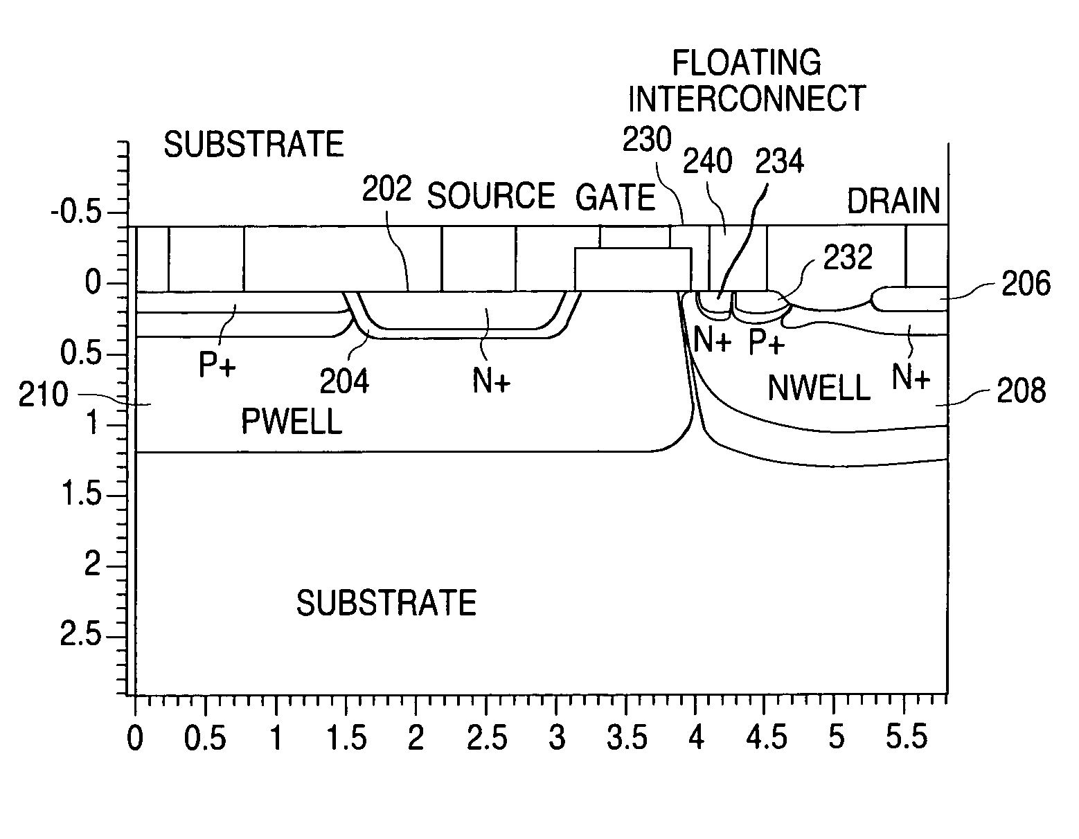
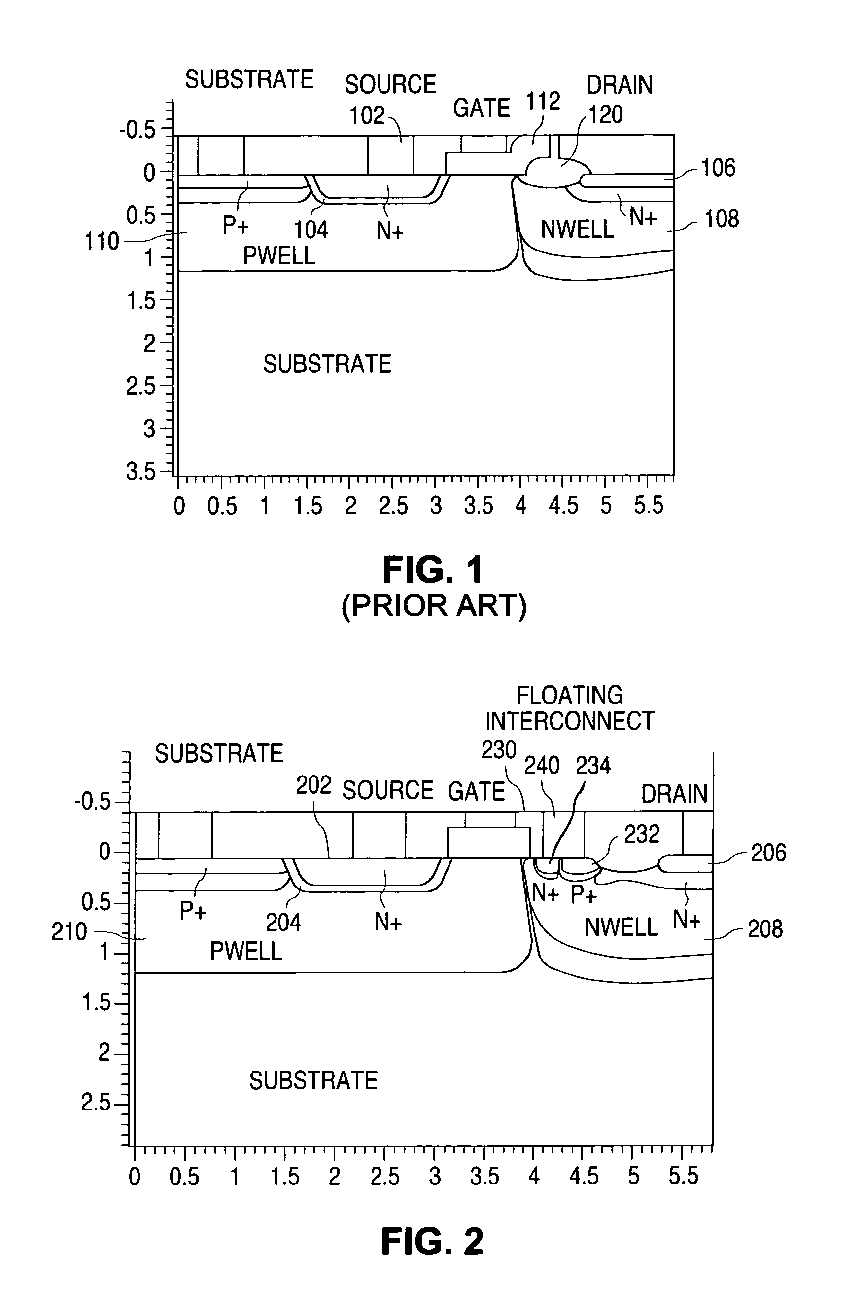
[0011]FIG. 2 shows one embodiment of the invention. As in the prior art LDMOS device of FIG. 1, the present embodiment of an LDMOS 200 has a source 202 formed in an n-well 204, and a drain 206 formed in an n-well 208. However, in accordance with the invention the thick field oxide 120 of the prior art, which reduces the surface field alongside the gate polysilicon, has been eliminated. This alleviates hot carrier degradation (HCD) since it eliminates a region that traps injected charge carriers. In order to create a reduced surface field (RESURF) in spite of the elimination of the thick field oxide the present embodiment introduces a p-doped region in the form of a p+ region 232 and a n-doped region in the form of a n+ region 234, alongside each other in the n-well 208. The p+ region 232 and n+ region 234 in this embodiment are shorted to each other by a floating interconnect 240, and the interconnect 240 is isolated from the polysilicon gate 212 by an oxide layer 230. Since the pre...


PUM


Abstract

In a method and structure for a high voltage LDMOS with reduced hot carrier degradation, the thick field oxide is eliminated and a reduced surface field achieved instead by including adjacent p+ and n+ regions in the drain well and shorting these regions to each other, or by including a p+ region in the drain well and biasing it to a positive voltage relative to the source voltage.

Description

FIELD OF THE INVENTION[0001]The invention deals CMOS / BiCMOS technologies. In particular it deals with extended voltage range devices.BACKGROUND OF THE INVENTION[0002]Numerous applications such as portable power supplies, amplifiers, EEPROMs, charge pumps on-chip, etc., need to be operated at higher voltage levels. These extended voltages typically range between 12V and 20V. In order to keep costs down is desirable to be able to use base 5V technology to build these high voltage devices, thereby avoiding having to resort to special high voltage technologies.[0003]One solution that makes use of only existing masks and thereby limits costs is the extended drain device, also sometimes referred to as lateral DMOS (LDMOS), illustrated in FIG. 1. The device 100 includes a source 102 formed in an n-well 104, and a drain 106 formed in an n-well 108. In order to accommodate the higher voltage levels the drain 106 is extended in length as shown in FIG. 1. Due to the high voltage applied to the...

Claims


Application Information

Patent Timeline
IPC IPC(8): H01L29/76
CPCH01L29/0619H01L29/7835H01L29/0847H01L29/0634H01L29/0878H01L29/086
Inventor VASHCHENKO, VLADISLAVHOPPER, PETER J.MIRGORODSKI, YURILINDORFER, PHILIPP
Owner NAT SEMICON CORP
Learn More