
Semiconductor device and method of operating the same and structure for suppressing current leakage

a semiconductor device and current leakage suppression technology, applied in the direction of semiconductor devices, basic electric elements, electrical appliances, etc., can solve the problem of isolation between adjacent transistors in the level shifter, and achieve the effect of improving the current leakage of the semiconductor devi

Active Publication Date: 2016-11-29
EPISIL TECH INC
View PDF11 Cites 0 Cited by
  • Summary
  • Abstract
  • Description
  • Claims
  • Application Information

AI Technical Summary

Benefits of technology

This invention provides a way to improve the current leakage and breakdown voltage of a semiconductor device. It does this by putting a layer of isolation and a layer of PN junction diode on the substrate, in the same area. This reduces the surface field effect and allows for better control of the electric field concentration. This structure not only increases the breakdown voltage but also helps to suppress current leakage.

Problems solved by technology

Isolation between adjacent transistors in the level shifters has been an issue that researchers in relevant industries are working on.

Method used


Image

  • Semiconductor device and method of operating the same and structure for suppressing current leakage
  • Semiconductor device and method of operating the same and structure for suppressing current leakage
  • Semiconductor device and method of operating the same and structure for suppressing current leakage

Examples


Embodiment Construction

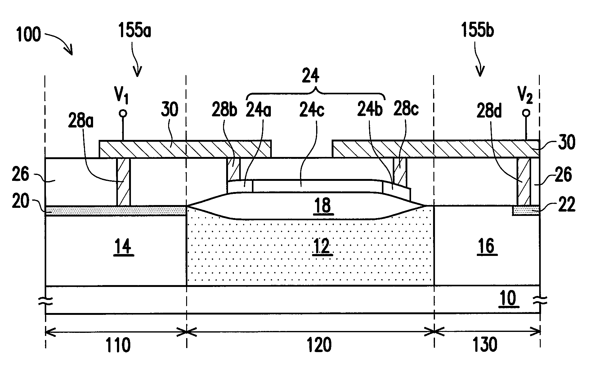
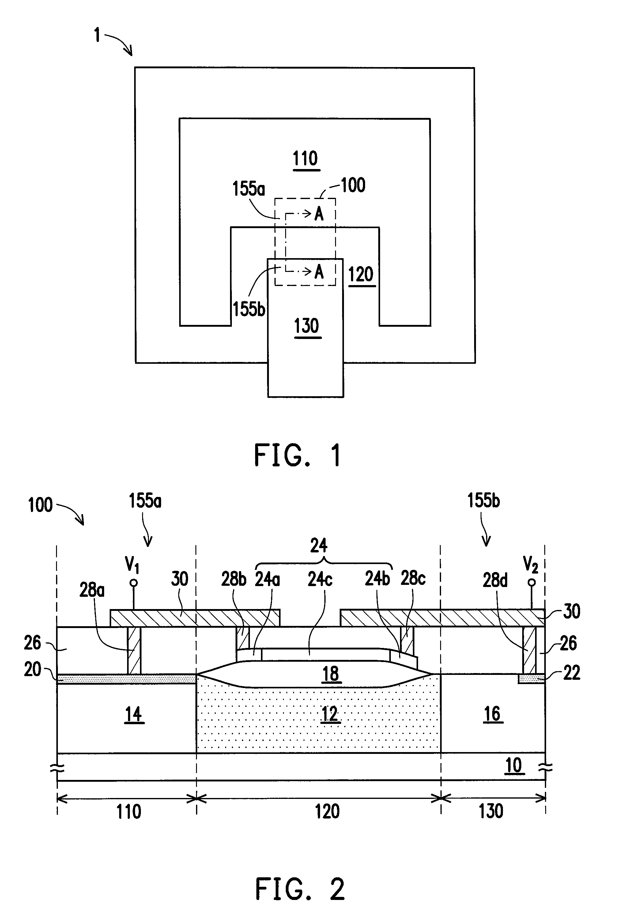
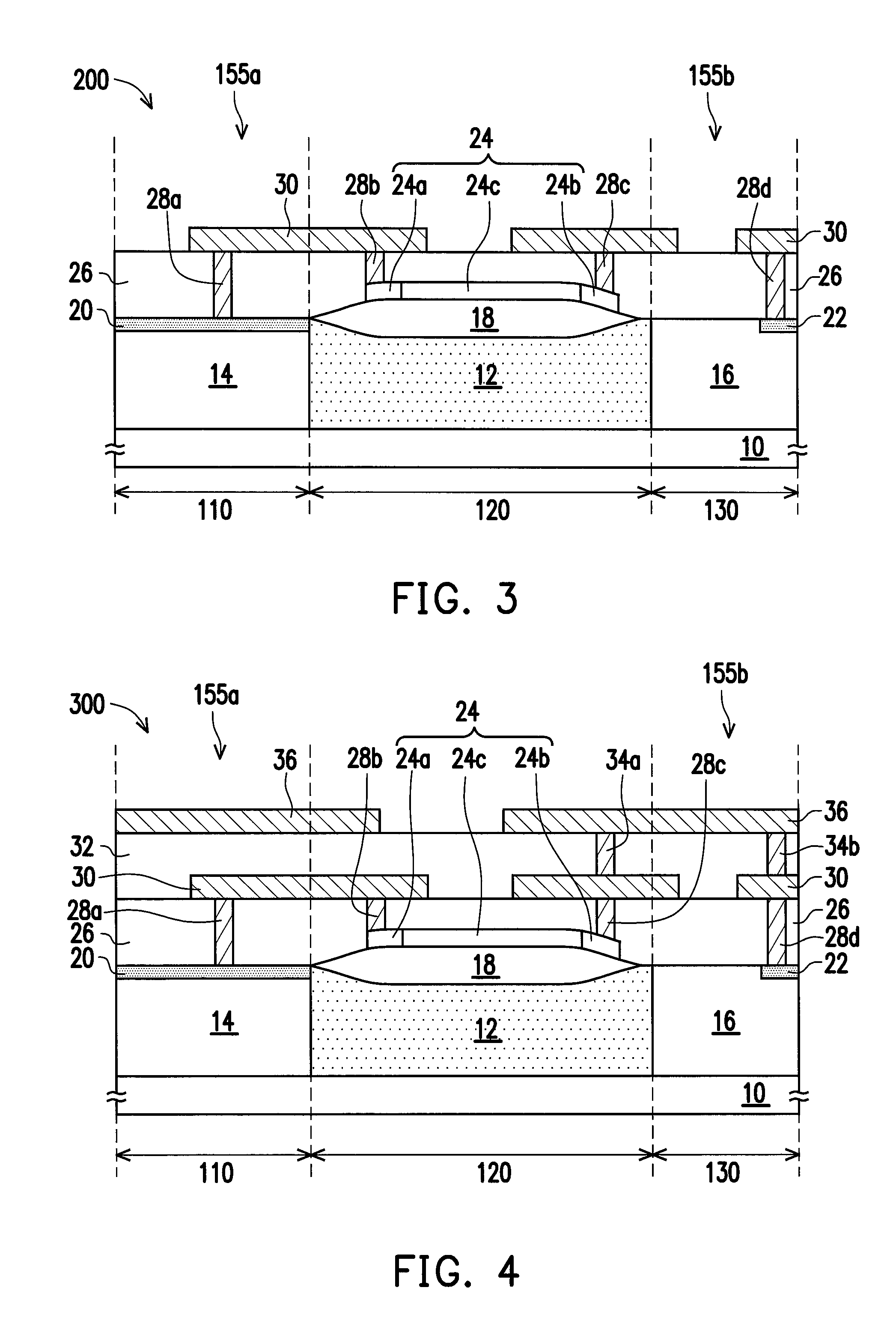
[0035]Reference will now be made in detail to the present preferred embodiments of the invention, examples of which are illustrated in the accompanying drawings. Wherever possible, the same reference numbers are used in the drawings and the description to refer to the same or like parts.

[0036]In the following embodiments, when a first conductivity type is N-type, a second conductivity type is P-type, and when the first conductivity type is P-type, the second conductivity type is N-type. The following embodiment is described by taking P-type as the first conductivity type and N-type as the second conductivity type. However, the invention is not limited thereto. The P-type dopant includes boron, and the N-type dopant includes phosphorous or arsenic.

[0037]FIG. 1 is a schematic top view illustrating a semiconductor device according to an embodiment of the invention.

[0038]A semiconductor device 1 of the invention has a first area 110, a second area 120, and a third area 130. The first ar...


PUM


Abstract

A structure for suppressing current leakage and a semiconductor device including the same are provided. The structure for suppressing current leakage includes a substrate of a first conductivity type, a well region of the first conductivity type, an isolation structure and a PN junction diode. The well region is disposed in the substrate. The isolation structure is disposed on the well region. The PN junction diode is disposed on the isolation structure and configured to suppress current leakage of the semiconductor device.

Description

CROSS REFERENCE TO RELATED APPLICATION[0001]This application claims the priority benefit of Taiwan application serial no. 103137000, filed on Oct. 27, 2014. The entirety of the above-mentioned patent application is hereby incorporated by reference herein and made a part of specification.BACKGROUND OF THE INVENTION[0002]1. Field of the Invention[0003]The invention relates to a semiconductor device, and particularly relates to a structure for suppressing current leakage and a semiconductor device including the structure for suppressing current leakage.[0004]2. Description of Related Art[0005]Recently, as people are gaining the awareness of environmental protection, high voltage power integrated circuits featuring low power consumption and high power conversion efficiency are drawing more and more attention. Generally speaking, the high voltage power integrated circuits are mainly used in power switch devices and applied in the fields of switching mode power supply (SMPS), luminaire, m...

Claims


Application Information

Patent Timeline
Patent Type & Authority Patents(United States)
IPC IPC(8): H01L29/00H01L29/06H01L29/861H01L29/40
CPCH01L29/0653H01L29/402H01L29/8611H01L29/8613H01L21/76H01L29/861H01L29/1608H01L29/2003H01L21/76202
Inventor WU, HSIAO-CHIATENG, DUN-JENDAI, CHI-JEI
Owner EPISIL TECH INC
Learn More