
Trench power MOSFET and fabrication method thereof

a technology fabrication method, which is applied in the direction of basic electric elements, electrical apparatus, and semiconductor devices, can solve the problems of increasing manufacturing complexity, reducing the manufacturing cost of power semiconductors, and wasting usable materials, so as to reduce the on resistance, increase the voltage withstanding capability of trench power mosfet, and reduce the effect of voltage withstanding design

Inactive Publication Date: 2014-10-28
SUPER GROUP SEMICON
View PDF5 Cites 0 Cited by
  • Summary
  • Abstract
  • Description
  • Claims
  • Application Information

AI Technical Summary

Benefits of technology

The present patent describes a trench power MOSFET (metal-oxide semiconductor field-effect transistor) that has multiple trenches in its termination region. These trenches extend outward from the active region and are filled with isolation layer and conductive material inside them. This design increases the voltage withstanding capability of the MOSFET while reducing its on resistance. It also reduces the required area for voltage withstanding design, thereby reducing manufacturing costs. In simple terms, this patent is about a new way to make power MOSFETs that are stronger and have lower resistance.

Problems solved by technology

Implementing the described guard ring structure not only may waste the usable wafer area but also increase the manufacturing complexity henceforth the manufacture cost of the power semiconductor may be substantially increased and thereby reduce the associated economic efficiency.
Thus, electric field with moderate electric field distribution may form on the side or bottom of trench producing the trench power MOSFET has high voltage withstanding capability and low on resistance.

Method used


Image

  • Trench power MOSFET and fabrication method thereof
  • Trench power MOSFET and fabrication method thereof
  • Trench power MOSFET and fabrication method thereof

Examples


first exemplary embodiment

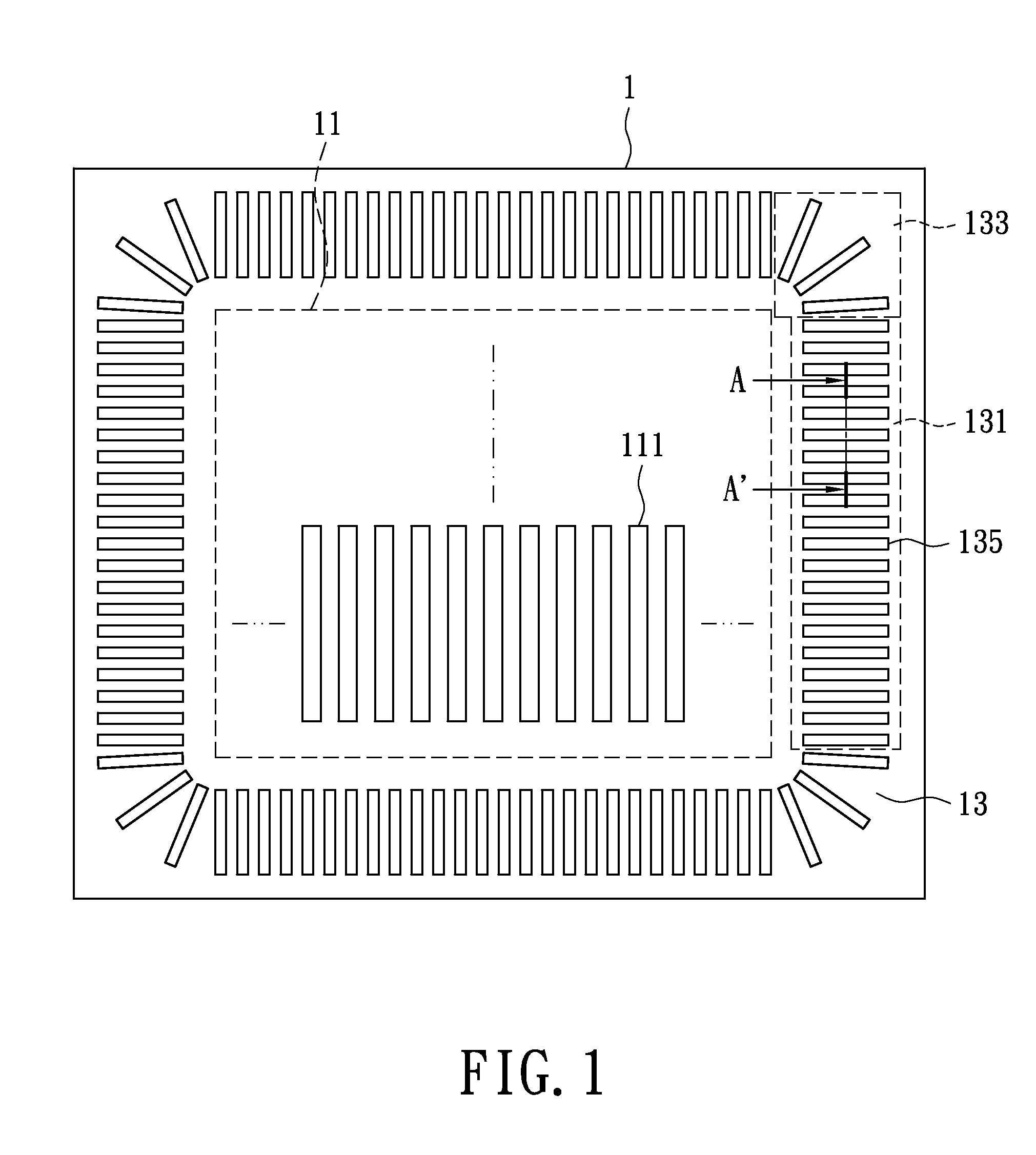
[0027]Please refer to FIG. 1, which shows a top view of a trench power MOSFET in accordance to the first exemplary embodiment of the present disclosure. The trench power MOSFET includes a substrate (not shown) and an epitaxial layer 1, a plurality of first trenches 111, and a plurality of second trenches 135 disposed thereon. The substrate and the epitaxial layer 1 collectively formed a base.

[0028]The epitaxial layer 1 in the instant embodiment may be grown on the substrate using the epitaxial growth technique. However, in other embodiment, the base may comprise of only the substrate that is the active region and the termination region may be directly formed on the substrate without the need to grow the epitaxial layer 1, hence the instant embodiment shall not be limited herein. It is worth to note that the substrate may be a silicon substrate having a first conductive type dopant. The drain region of the trench power MOSFET is disposed on the bottom of the substrate. In practice, t...

second exemplary embodiment

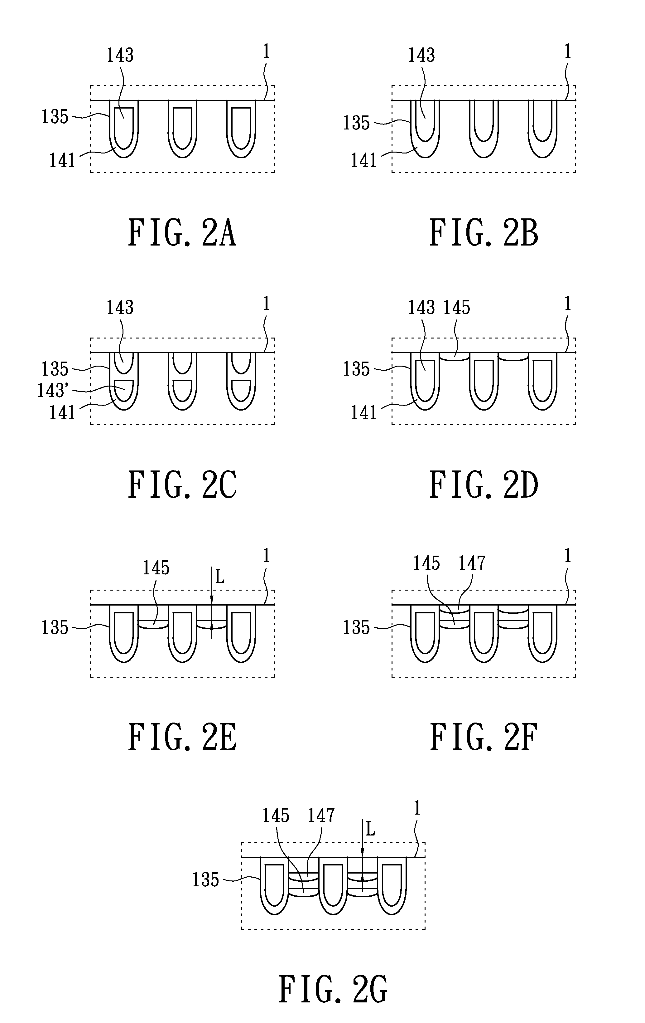
[0045]In addition, the placement of the first dopant region 145 may have other implementation. Please refer to FIG. 3A and FIG. 3B, which respectively show diagrams illustrating a first and a second doped region distribution associated with the trench power MOSFET in accordance to the second exemplary embodiment of the present disclosure.

[0046]As shown in FIG. 3A, the first dope region 145a having dopant with conductive type different from the epitaxial layer 1 may be implanted substantially in the central region between the adjacent second trenches 135. The length of the first dopant region 145a falls within the trench length of the second trench 135. However, the instant disclosure is not limited thereby, as the length of the first dopant region 145a may be greater or equal to the trench length of the second trench 135. The maximum width of the first dopant region 145a is defined by the gap size between the adjacent second trenches 135. The first dopant region 145 can be disposed ...

third embodiment

[0050]Please refer FIG. 4A and FIG. 4B which respectively show diagram illustrating method of metal layer deposition in accordance to the third exemplary embodiment of the present disclosure.

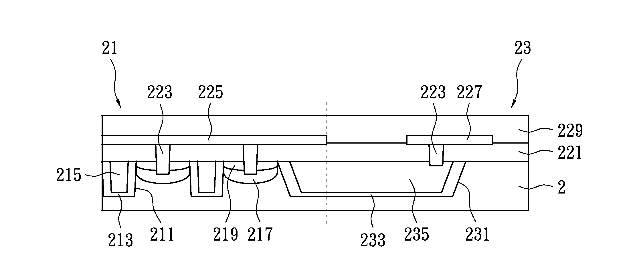
[0051]The metal layer 139 may electrically connect to the plurality of the second trenches 135 through the corresponding plurality of contact via 137. As shown in FIG. 4A, a plurality of contact vias 137 are respectively formed by vertically downward etching the surface of epitaxial layer 1 in corresponding to the placement of the second trenches 135 within the terminal region (not shown in FIGS. 4A and 4B). So that the contact vias 137 are electrically connected to the conductive structures (not shown in FIGS. 4A and 4B) formed by conductive material filled in the second trenches 135. Each of the second trenches 135 may electrically connect to the metal layer 139 through at least one contact via 137. Alternatively, the metal layer 139 may through the contact vias 137 electrically connect to the...


PUM


Abstract

An exemplary embodiment of the present disclosure illustrates a trench power MOSFET which includes a base, a plurality of first trenches, and a plurality of second trenches. The base has an active region and a termination region, wherein the termination region surrounds the active region. The plurality of first trenches is disposed in the active region. The plurality of second trenches is disposed in the termination region, wherein the second trenches extend outward from the active region side. The second trenches have isolation layers and conductive material deposited inside, in which the isolation layers are respectively disposed in the inner surface of the second trenches. The disclosed trench power MOSFET having the second trenches disposed in the termination region can increase the breakdown voltage thereof while minimize the termination region area thereby reduce the associated manufacturing cost.

Description

BACKGROUND[0001]1. Technical Field[0002]The present disclosure relates to a semiconductor structure and the fabrication method thereof in particular, to trench power metal oxide semiconductor field effect transistor (MOSFET) and fabrication method thereof.[0003]2. Description of Related Art[0004]In order to fulfill energy saving and power consumption reduction requirements, power semiconductor devices e.g., power MOSFETs have been widely utilized in high voltage equipment. In the field of power semiconductor, the voltages withstanding capability (e.g., breakdown voltage BVdss) and conductivity characteristics (on resistance Ron) are known to be the most important capability indices for the power semiconductors.[0005]In practice, to increase the breakdown voltage of a power semiconductor, at least a guard ring structure consisting of a p-n junction formed of a P-type semiconductor and an N-type semiconductor and a metal formed field plate is disposed on the wafer surrounding the powe...

Claims


Application Information

Patent Timeline
Patent Type & Authority Patents(United States)
IPC IPC(8): H01L29/66
CPCH01L29/42368H01L29/7813H01L29/66727H01L29/0696H01L29/0878H01L29/0619H01L29/66734H01L29/7811H01L29/41766H01L29/0623H01L29/407
Inventor YEH, CHUN-YINGLEE, YUAN-MING
Owner SUPER GROUP SEMICON
Learn More