Lead frame with plated end leads

a lead frame and end lead technology, applied in the direction of printed circuit manufacturing, sustainable manufacturing/processing, final product manufacturing, etc., can solve the problems of reducing the solder joint strength, failure of one or more of the solder joints, and worst board level performance, so as to facilitate the reflow of solder, increase the overall solder joint strength and reliability, and increase the solderable area

Inactive Publication Date: 2007-02-27
AMKOR TECH SINGAPORE HLDG PTE LTD
View PDF211 Cites 99 Cited by
  • Summary
  • Abstract
  • Description
  • Claims
  • Application Information

AI Technical Summary

Benefits of technology

[0012]In accordance with the present invention, there is provided a lead frame which comprises a frame defining a central opening. Disposed within the central opening is a die pad which is connected to the frame. Also connected to the frame are a plurality of leads which extend within the opening toward the die pad. Each of the leads defines opposed top and bottom surfaces, an inner end, an outer end, and an opposed pair of side surfaces. The bottom surface and the outer end collectively define a corner region of the lead. Formed within the corner region is a recess. The recesses facilitate the reflow of solder up the lead ends, thereby increasing the overall solder joint strength and reliability between the semiconductor package incorporating the lead frame and an underlying substrate such as a printed circuit board or motherboard. The surfaces of the lead defining the recess are plated, with the inclusion of the recess within each lead effectively increasing the solderable area of the leads of the semiconductor package to the printed circuit board, with the final solder joint being stronger with increased second level reliability.

Problems solved by technology

However, the limited solderable area on the MLF package and resultant decreased solder joint strength gives rise to reliability problems concerning the potential failure of one or more of the solder joints between the MLF package and the motherboard.
However, material sets which give the best package level performance may also produce the worst board level performance, thus necessitating another option to increase overall solder strength and reliability between the MLF package and the motherboard.
Saw generated burrs at the seating plan of each lead in the lead frame adversely affect solder mounting and joint reliability.

Method used


Image

  • Lead frame with plated end leads
  • Lead frame with plated end leads
  • Lead frame with plated end leads

Examples


Embodiment Construction

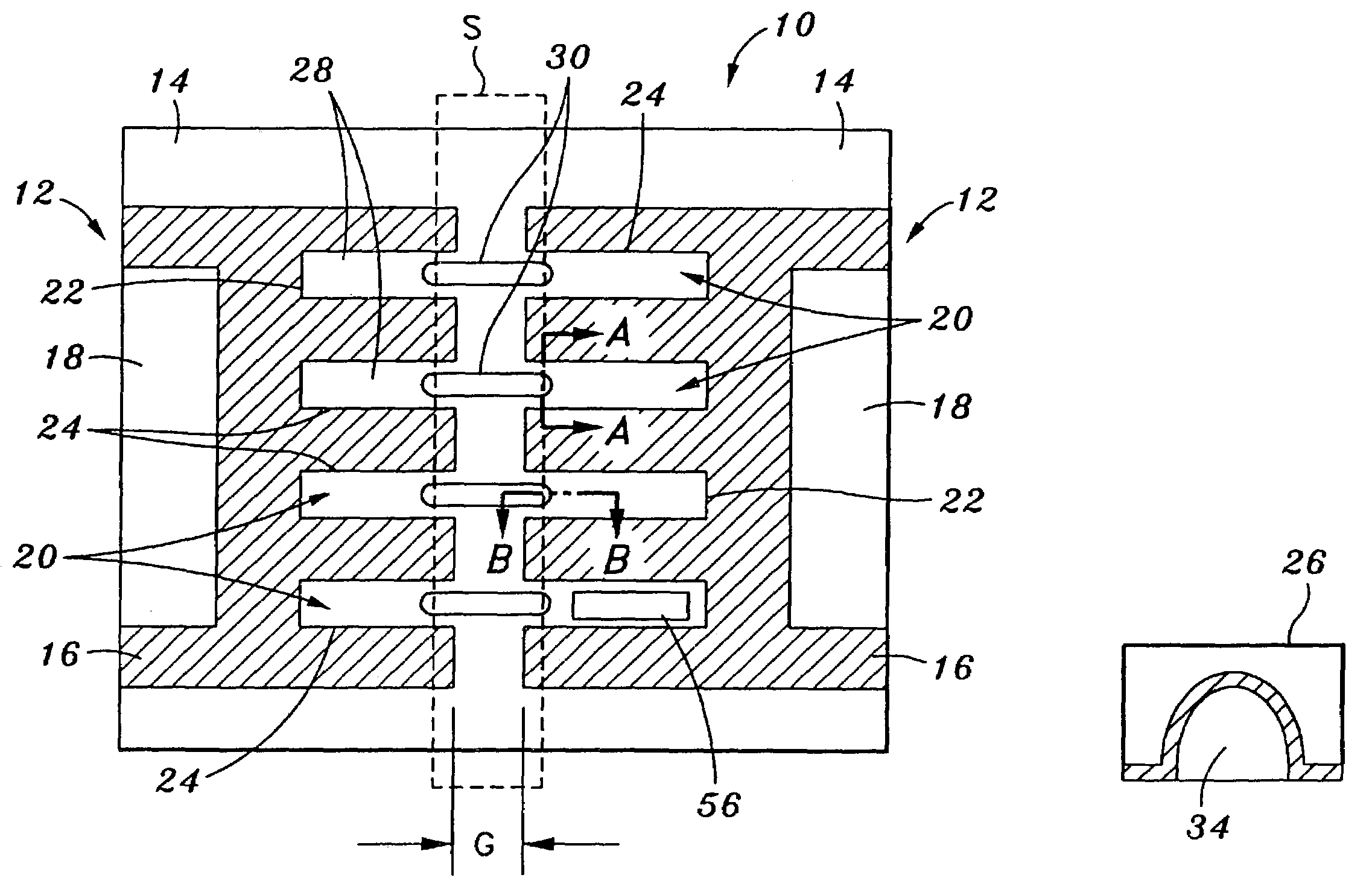
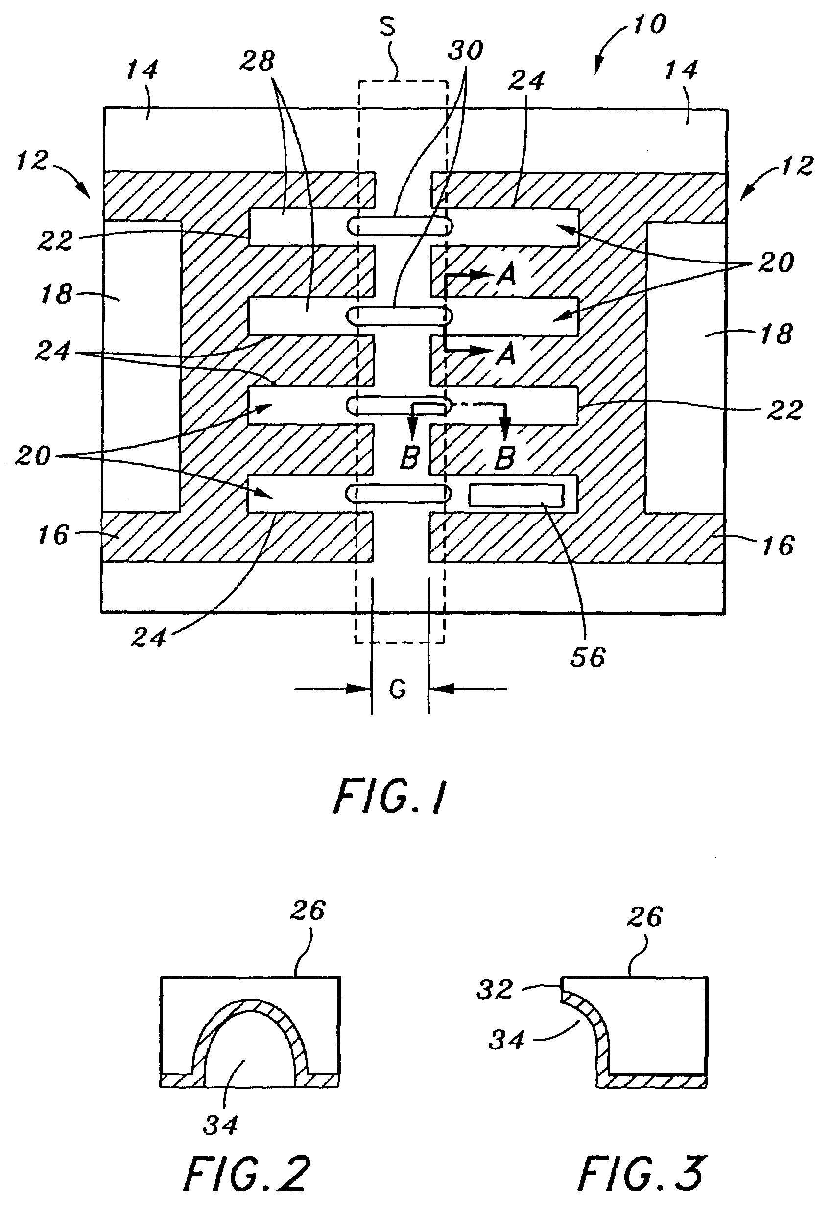
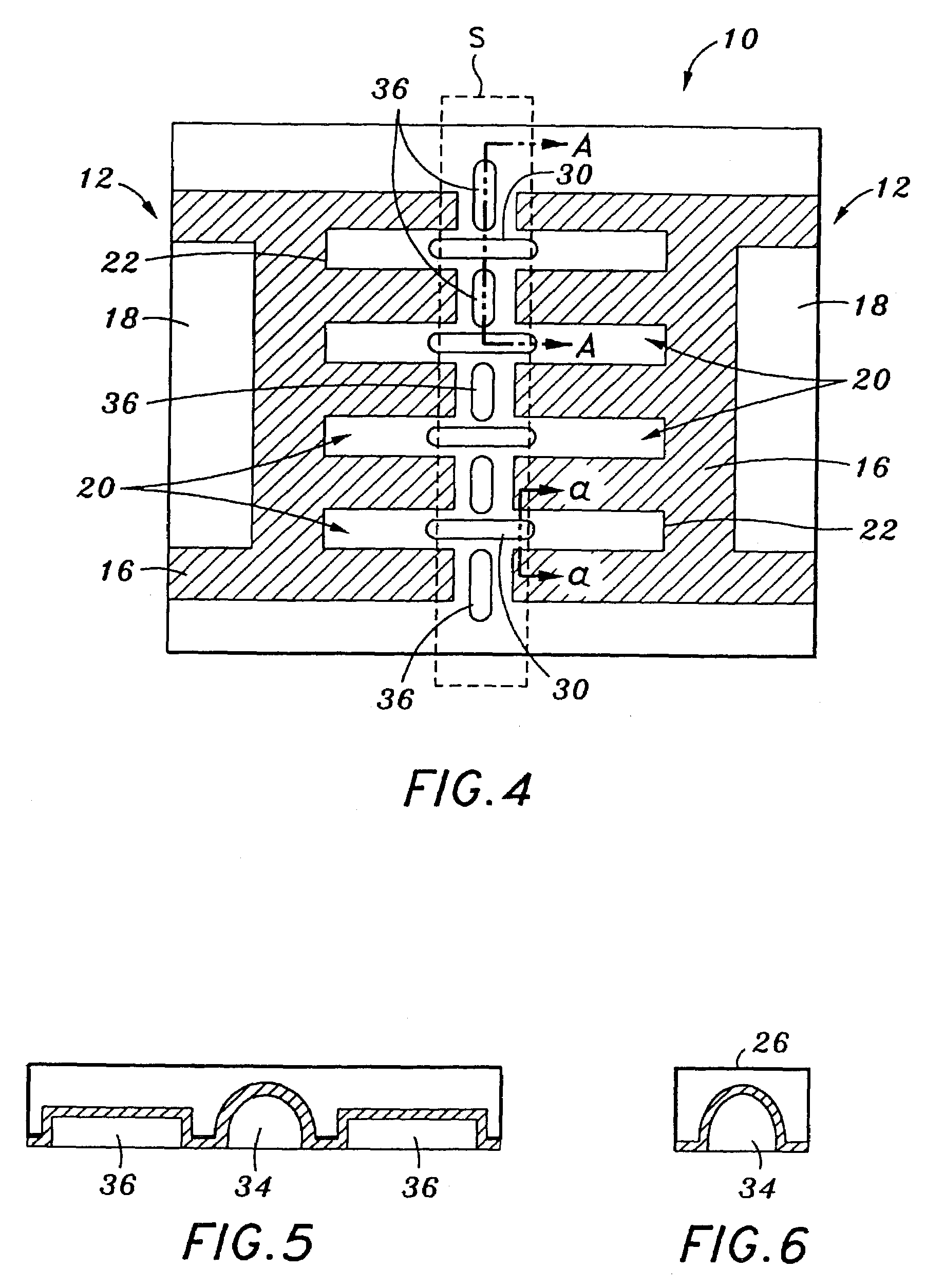
[0034]Referring now to the drawings wherein the showings are for purposes of illustrating preferred embodiments of the present invention only, and not for purposes of limiting the same, FIG. 1 depicts a lead frame strip 10 which is uniquely configured to facilitate the production of a multiplicity of lead frames 12 which are each formed in accordance with the present invention. The strip 10 has a generally rectangular configuration, defining opposed pairs of longitudinal and lateral peripheral edge segments. The strip 10 is typically formed to define multiple, identically configured arrays, with a portion of one such array being shown in FIG. 1. Each array defines a multiplicity of the lead frames 12.

[0035]Each lead frame 12 comprises an outer frame portion 14 which defines a centrally positioned opening 16. Disposed within the opening 16 is a die pad 18 of the lead frame 12. Though not shown in FIG. 1, the die pad 18 is typically connected to the outer frame portion 14 by a plurali...


PUM


Abstract

A lead frame comprising a frame which defines a central opening. Disposed within the central opening is a die pad which is connected to the frame. Also connected to the frame are a plurality of leads which extend within the opening toward the die pad. Each of the leads defines opposed top and bottom surfaces, an inner end, an outer end, and an opposed pair of side surfaces. The bottom surface and the outer end collectively define a corner region of the lead. Formed within the corner region is a recess which is sized and configured to accommodate the flow of reflow solder thereinto.

Description

RELATED APPLICATIONS[0001]The present application is a continuation of U.S. application Ser. No. 10 / 122,598 entitled LEAD FRAME WITH PLATED END LEADS AND RECESSES filed Apr. 15, 2002 now U.S. Pat. No. 6,608,366.STATEMENT RE: FEDERALLY SPONSORED RESEARCH / DEVELOPMENT[0002](Not Applicable)BACKGROUND OF THE INVENTION[0003]The present invention relates generally to integrated circuit chip package technology, and more particularly to a unique lead frame design for a micro lead frame (MLF) package wherein a special plated half-etched feature is included in the lead frame design which increases the solderable area of the leads of the lead frame to a printed circuit board, thus creating stronger final solder joints with increased second level reliability.[0004]Integrated circuit dies are conventionally enclosed in plastic packages that provide protection from hostile environments and enable electrical interconnection between the integrated circuit die and an underlying substrate such as a pr...

Claims


Application Information

Patent Timeline
Patent Type & Authority Patents(United States)
IPC IPC(8): H01L23/495H01L21/56H01L21/68H01L23/31H05K3/34
CPCH01L21/561H01L21/568H01L23/3107H01L23/49548H01L23/49582H05K3/3426H01L2924/0002H01L2924/00Y02P70/50H05K3/3431
Inventor FOGELSON, HARRY J.BANCOD, LUDCVICO ESTRADASYED, AHMERDAVIS, TERRYPALASI, PRIMITIVO A.ANDERSON, WILLIAM M.
Owner AMKOR TECH SINGAPORE HLDG PTE LTD
Why Eureka
Try Eureka