

Triple inverter pierce oscillator circuit suitable for CMOS
a technology of oscillator circuit and inverter, which is applied in the field of oscillator circuit, can solve the problems of resistive feedback and significantly reduce the overall gain of the three inverter stages, and achieve the effect of preventing any parasitic oscillation
- Summary
- Abstract
- Description
- Claims
- Application Information
AI Technical Summary
Benefits of technology
Problems solved by technology
Method used
Image

Examples
Embodiment Construction
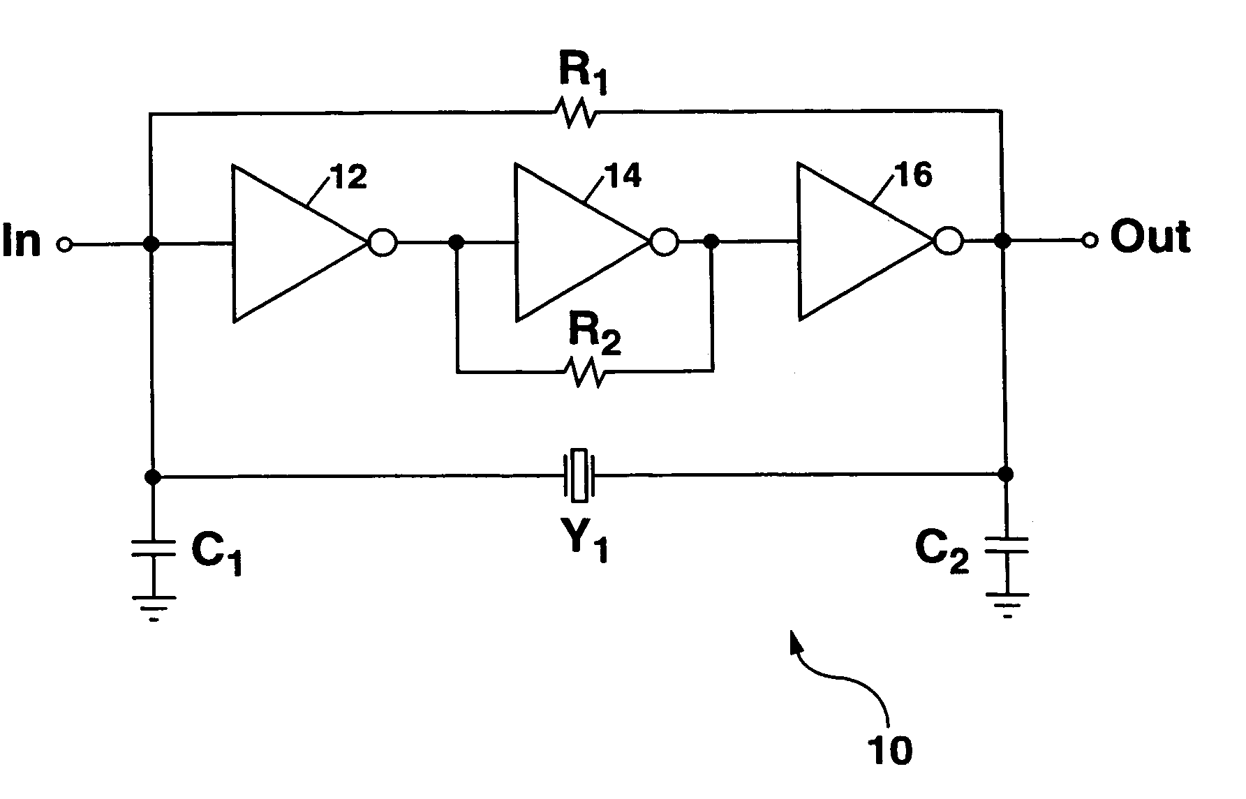
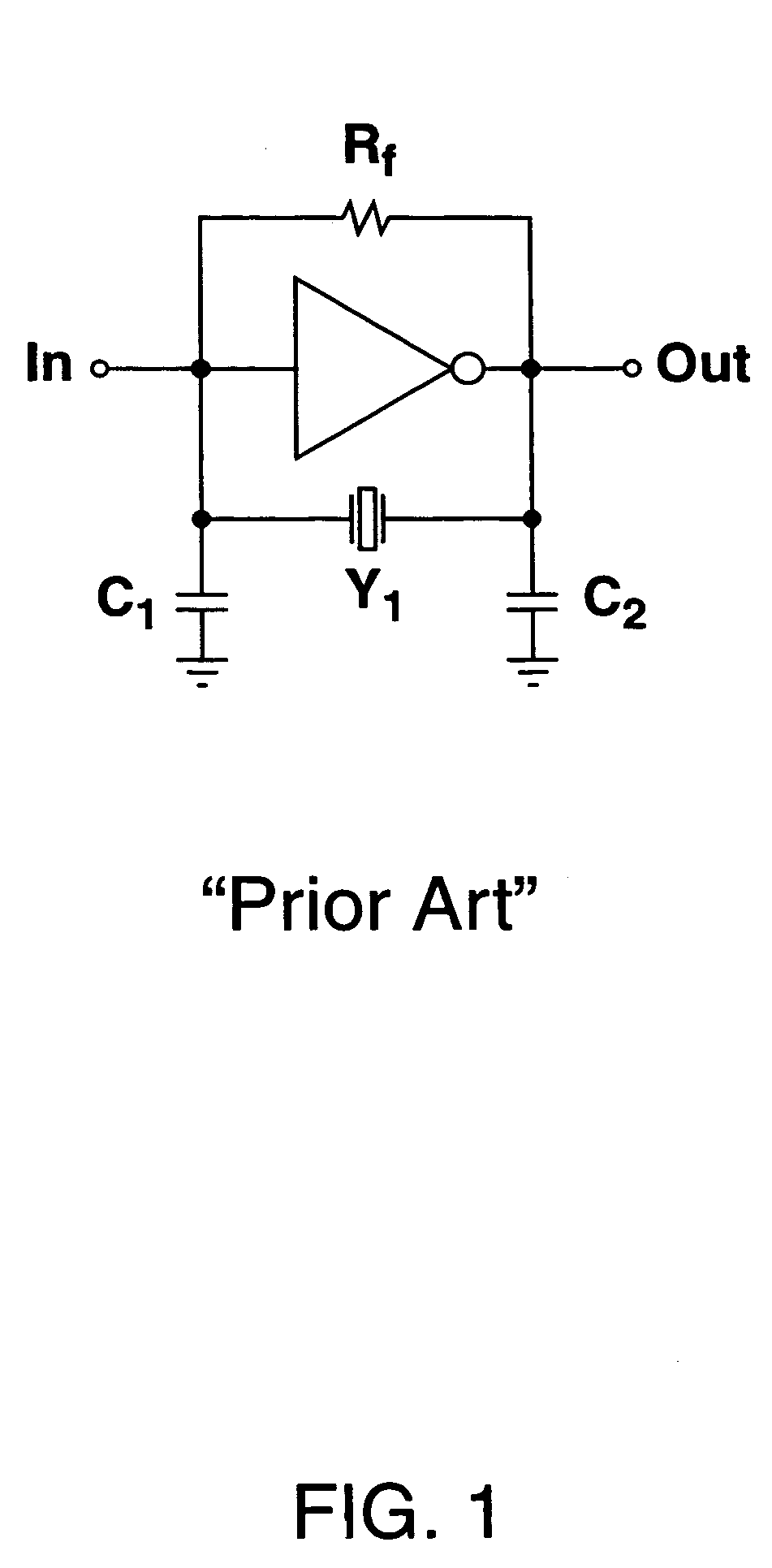
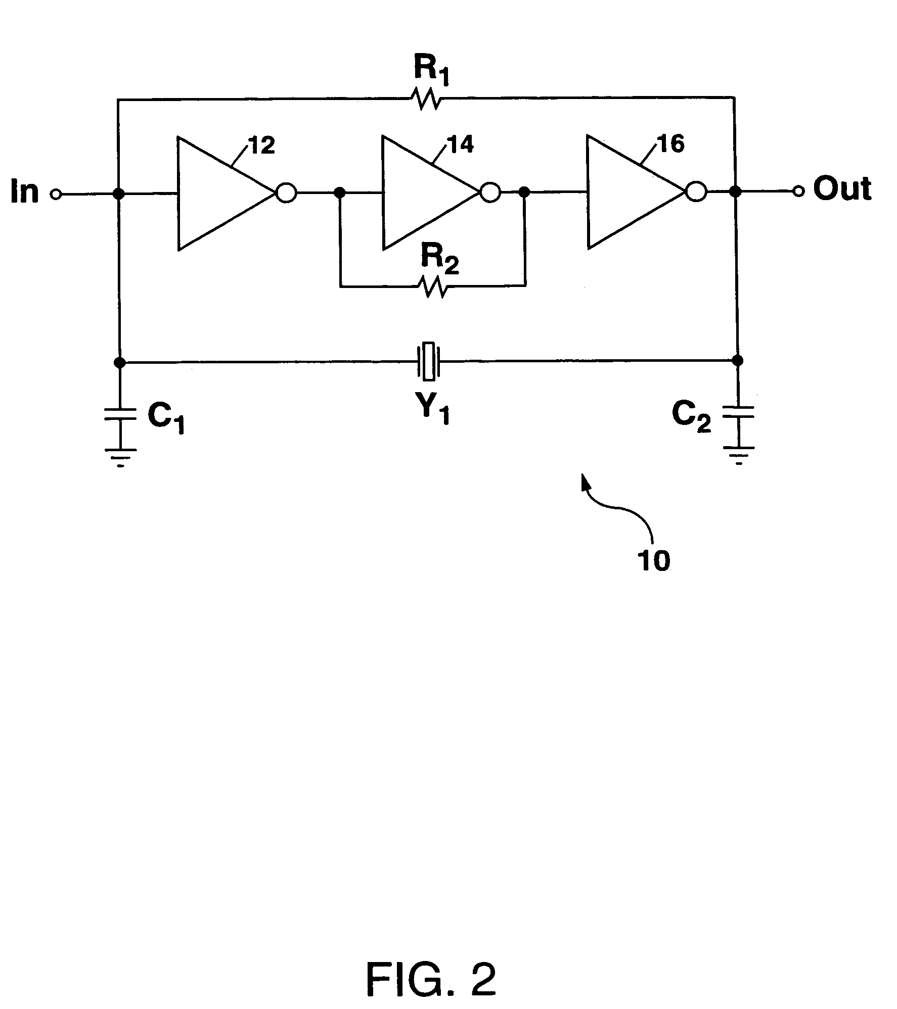
[0033]Referring to FIG. 1, there is shown a single-inverter Pierce oscillator circuit as known in the prior art. The oscillator circuit of FIG. 1 utilizes a single inverter which can be implemented using N-channel and P-channel field-effect transistors (FETs). A resonator Y1 is embedded between two capacitors C1 and C2 and further connected between the output of the circuit and the input thereof to provide a feedback path for oscillation at an oscillation frequency which is defined by the resonator Y1. A feedback resistor Rf, with a value in the range from 100 kΩ up to a few megaOhms (MΩ), is provided between the input and output of the oscillator circuit to bias the oscillator circuit for start-up.
[0034]The single-inverter Pierce oscillator circuit of FIG. 1 works relatively well for relatively-high-transconductance FETs, and for a relatively low-frequency, low-loss resonator Y1. Additionally, the capacitors C1 and C2 must be carefully chosen to provide for adequate excess loop gai...
PUM
 Abstract
Description
Claims
Application Information