Portable device

a technology of portable devices and coaxial cables, applied in the direction of instruments, optical waveguide light guides, optical elements, etc., can solve the problems of speech quality and calling reliability, limit the achievable signal transmission speed, increase the number of coaxial cables, etc., and achieve the effect of improving portability

Active Publication Date: 2007-02-27
PANASONIC CORP
View PDF12 Cites 27 Cited by
  • Summary
  • Abstract
  • Description
  • Claims
  • Application Information

AI Technical Summary

Benefits of technology

[0019]The other object of the present invention is to provide a portable device having such a configuration that a plurality of housings are connected functionally, wherein the thickness of a connection section between the housings is reduced so that the portability is improved.

Problems solved by technology

This places a limit to the increase in the number of coaxial cables, and hence has caused a limit to the achievable signal transmission speed.
Further, electromagnetic interference in the electric signals occurs between the antenna and the coaxial cables in the hinge portion, and thereby has caused a problem in speech quality and calling reliability.
Nevertheless, in the case of optical fibers disclosed in patent document 1, when the optical fibers are made of glass, the fibers break and become disconnected when their bend radius becomes small.
That is, when the fold-up portion is closed, or in the course of the folding up, high speed transmission is not achieved.
This places a notable restriction on the use of the device.
In order to reduce this optical loss, when the fibers made of plastics were constructed such as to be bent in a larger bend radius, the device thickness in a folded-up state could increase so as to cause a problem in the portability.
That is, the film-shaped optical waveguides are not expected to be extremely bent or folded up into a bend radius of as small as 5 mm or even less, as is the case with a portable device.
Thus, when the bend radius becomes small, the optical loss increases.
Thus, as a whole, thickness reduction is not sufficiently achieved in the connection section.

Method used


Image

  • Portable device
  • Portable device
  • Portable device

Examples


embodiment 1

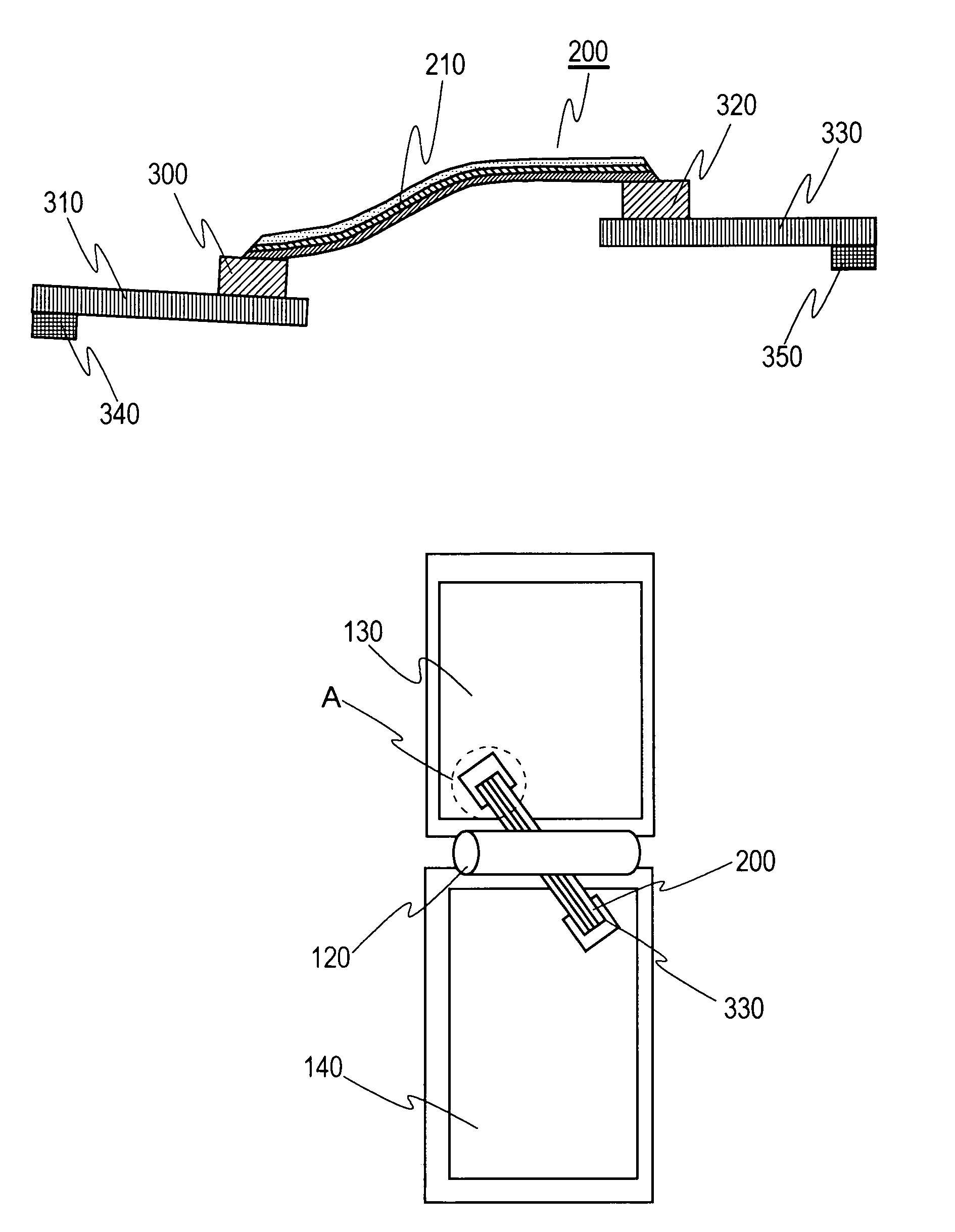
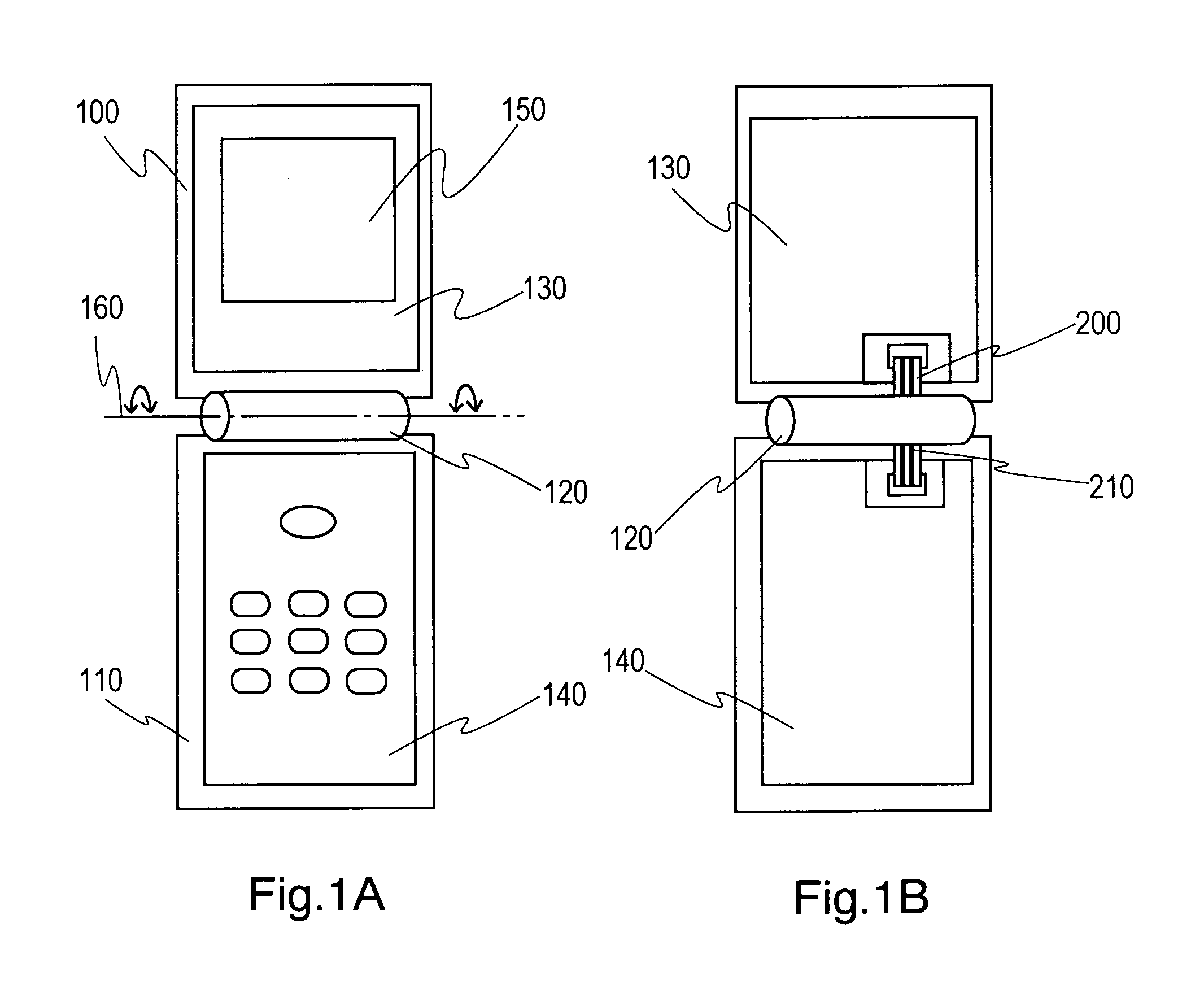
[0071]FIG. 1 is a schematic configuration diagram of a portable device according to Embodiment 1. FIG. 1A is a general view of the portable device, while FIG. 1B is a conceptual diagram showing the arrangement of an optical waveguide film in a connection section between a first housing and a second housing. It should be noted that an exterior is provided in practice for covering the connection section. However, in order to clearly show the arrangement of an optical waveguide film, the exterior is omitted in all the drawings including FIG. 1B.

[0072]The following description is given using a general portable phone as an example of a portable device. However, its basic structure is common also to portable devices such as a notebook personal computer and a PDA (Personal Digital Assistance) capable of being opened and closed freely.

[0073]In FIG. 1A, a first housing 100 and a second housing 110 are connected through a connection section 120 having a hinge capable of being opened and close...

embodiment 2

[0111]FIG. 10 is a schematic configuration diagram of a portable device according to Embodiment 2. FIG. 10A is a general view of the portable device. FIG. 10B is a conceptual diagram showing the arrangement of an optical waveguide film 200 in the connection section 120 for optically connecting the first housing 100 with the second housing 110. This configuration is the same as Embodiment 1 except that at least the optical waveguides 210 in the optical waveguide film 200 are arranged obliquely relative to the pivot axis 160 of the connection section 120.

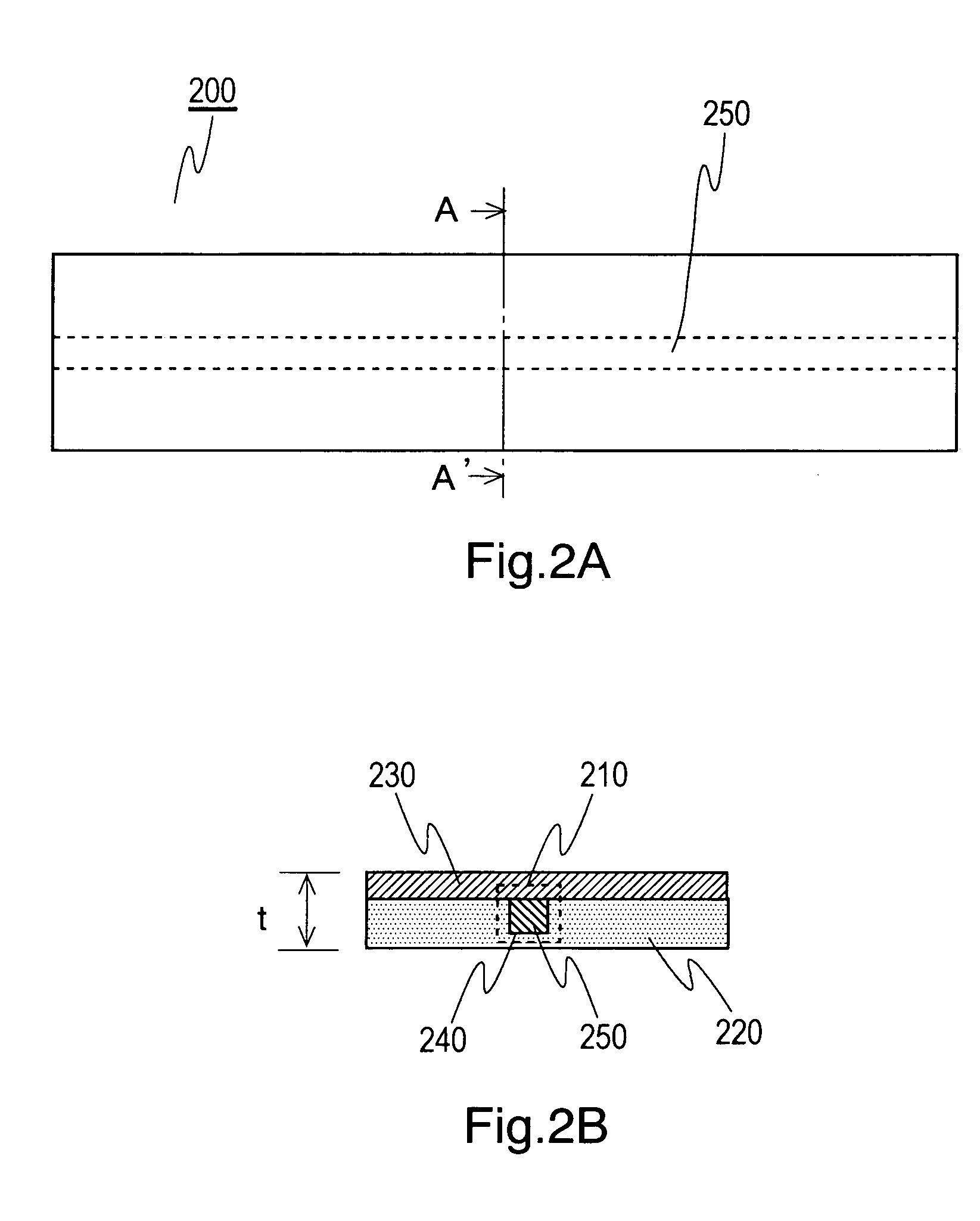
[0112]Embodiment 2 achieves further thickness reduction in a portable device according to Embodiment 1. The reason for this is described below. Table 1 shows the relative optical loss generated by bending of the optical waveguide film 200 as a function of the helix angle Φ (see FIG. 11A) between the pivot axis 160 of the connection section 120 and the optical waveguide 210 and using the thickness of the optical waveguide film 200 as a...

embodiment 3

[0122]FIG. 13 is a transparent perspective view showing the shape of an optical waveguide film used in a portable device according to Embodiment 3. This configuration is the same as Embodiment 1 except that the shape of the optical waveguide film 200 near the opening and closing of the connection section 120 is formed as an already bent shape 460.

[0123]Embodiment 3 reduces further the optical loss caused by the bending stress in the optical waveguide film 200 used in a portable device according to Embodiment 1. The reason for this is described below. As described in Embodiment 1, the mechanism of the optical loss caused by bending is that material distortion caused by the bending stress generates a change in the relative index difference of the core and the clad. That is, in the folding operation of the portable device, if the stress in the optical waveguide film 200 is minimum in an opened state, the generated stress reaches the maximum in a folded-up state (corresponding to 180° b...


PUM


Abstract

A portable device has a configuration such that a plurality of housings are connected functionally, wherein the thickness of a connection section between the housings is reduced so that the portability is improved. The portable device includes a first housing; a first board provided in the first housing; a second housing; a second board provided in the second housing; a connection section for connecting the first housing with the second housing in such a manner that their relative position can be changed; and an optical waveguide film having at least one optical waveguide for connecting the first board with the second board through optical wiring.

Description

CROSS-REFERENCE TO RELATED APPLICATION[0001]This application is based on Application Nos. 2004-184714 and 2004-070783 filed in Japan, the contents of which are hereby incorporated by reference.BACKGROUND[0002]1. Technical Field[0003]The present invention relates to a portable device and, in particular, to a portable device such as a portable phone, a PDA (Personal Digital Assistance), and a notebook personal computer, provided with a connection section for connecting a plurality of housings in such a manner that their relative position can be changed.[0004]2. Description of the Background Art[0005]In recent years, in portable devices such as portable phones, PDAs, and notebook personal computers, compact and thin devices are strongly desired for the easiness of carrying. Thus, in portable phones and notebook personal computers, such devices are commonly used that a plurality of housings can be folded up through a hinge portion of a thickness of 10 mm or the like so that portability ...

Claims


Application Information

Patent Timeline
Patent Type & Authority Patents(United States)
IPC IPC(8): G02B6/00G02B6/12G02B6/10G02B6/36H04B1/38H04M1/02H05K1/02
CPCG02B6/1221G02B6/3608G02B6/43G02B6/4214H04M1/0214G02B6/4224
Inventor KORENAGA, TSUGUHIROHIBINO, KUNIOITOH, NOBUKISHIMADA, MIKIHIROTOMITA, YOSHIHIRONAKAGIRI, YASUSHITOMEKAWA, SATORUKARASHIMA, SEIJI
Owner PANASONIC CORP
Why Eureka
Try Eureka