Method for production of MRAM elements

a technology of magnetoresistive elements and production methods, applied in semiconductor devices, digital storage, instruments, etc., can solve the problems of image distortion and instabilities, photolithography is susceptible, etc., and achieves the most repeatable method, the effect of easy repeatability in the deposition system

Inactive Publication Date: 2007-03-13
MICRON TECH INC
View PDF31 Cites 84 Cited by
  • Summary
  • Abstract
  • Description
  • Claims
  • Application Information

AI Technical Summary

Benefits of technology

[0011]According to a preferred embodiment, the invention relies on preferential patterning or roughening of the starting substrate surface, which patterning translates to magnetic alignment within the MRAM structure itself. The magnetic moments of ferromagnetic films produced according to the present invention will align preferentially along grooves or patterns generated in the starting surface. By generating very fine surface patterns, anisotropy is induced independent of the overall shape of the element, even if the element is circular or symmetric. This method allows control of the anisotropy or switching field to be generated by processes which are more reliable than photoiimaging.
[0013]Texturing an underlayer (seed layer) currently is preferred as the easiest and most repeatable method for inducing a secondary anisotropy in a magnetic film. This can be accomplished by utilizing off axis angular deposition which creates ripples by generating shadow effects as the film grows. The geometry and roughness that induce the anisotropy are controlled by deposition angle and thickness, which are very easy to repeat in a deposition system.

Problems solved by technology

Photolithography is susceptible, however, to image distortion and instabilities, problems that are exacerbated at the sub-micron level at which magnetic memory elements are being manufactured.

Method used


Image

  • Method for production of MRAM elements
  • Method for production of MRAM elements
  • Method for production of MRAM elements

Examples


Embodiment Construction

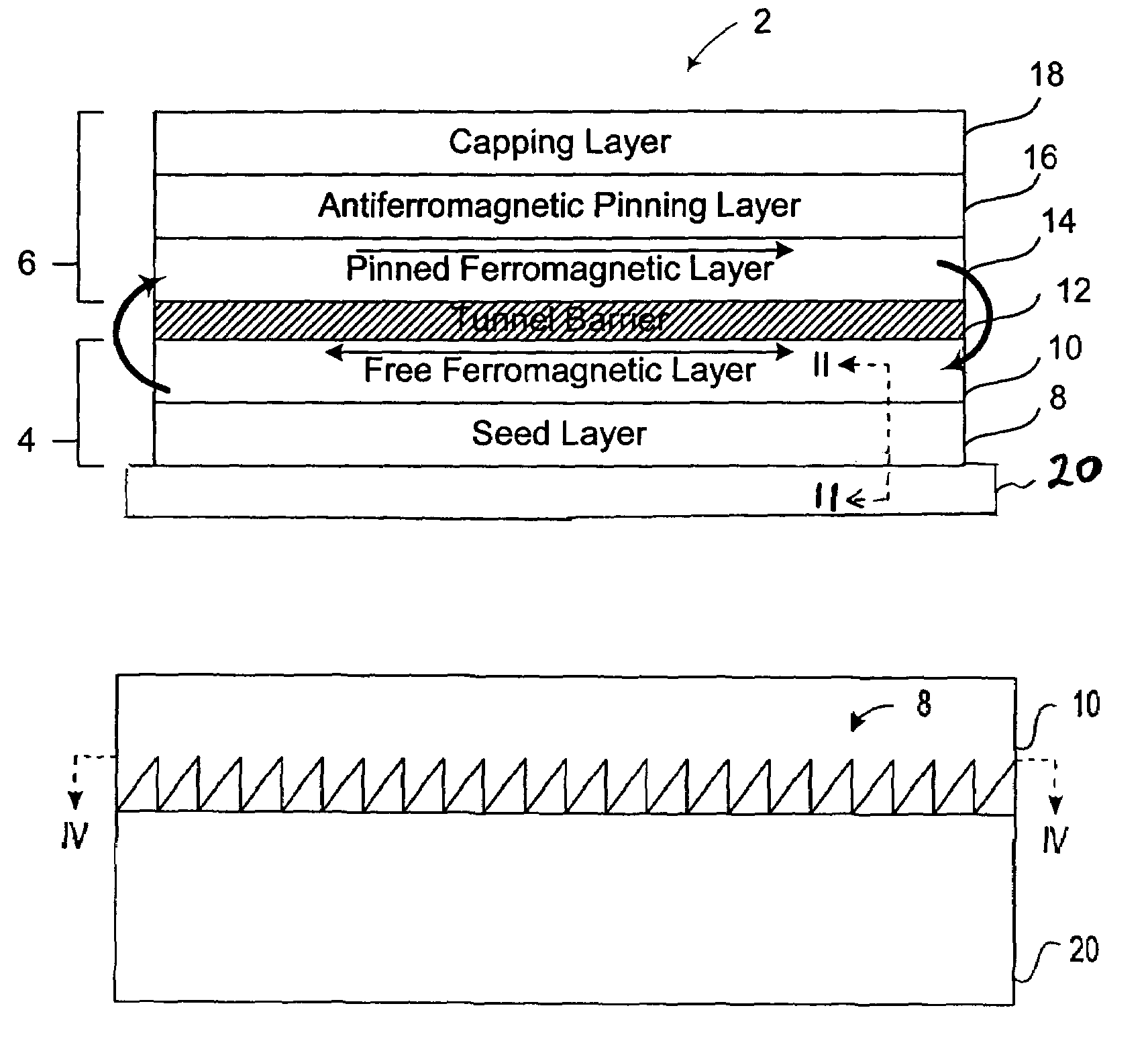
[0020]A generalized, exemplary magneto-resistive element structure 2 is shown in FIG. 1. The structure includes a free stack 4 and a pinned stack 6 formed above a substrate 20. Free stack 4 includes a seed layer 8 on which is disposed a free ferromagnetic layer 10. Above free stack 4 is pinned stack 6, separated by a tunnel barrier layer 12. Pinned stack 6 is made up of a pinned ferromagnetic layer 14, an antiferromagnetic pinning layer 16, and a capping layer 18. Other arrangements can be used. For example, the free and pinned ferromagnetic layers 10 and 14 may each be formed as a plurality of stacked individual layers. The stacks also can include offset control and coupling layers.

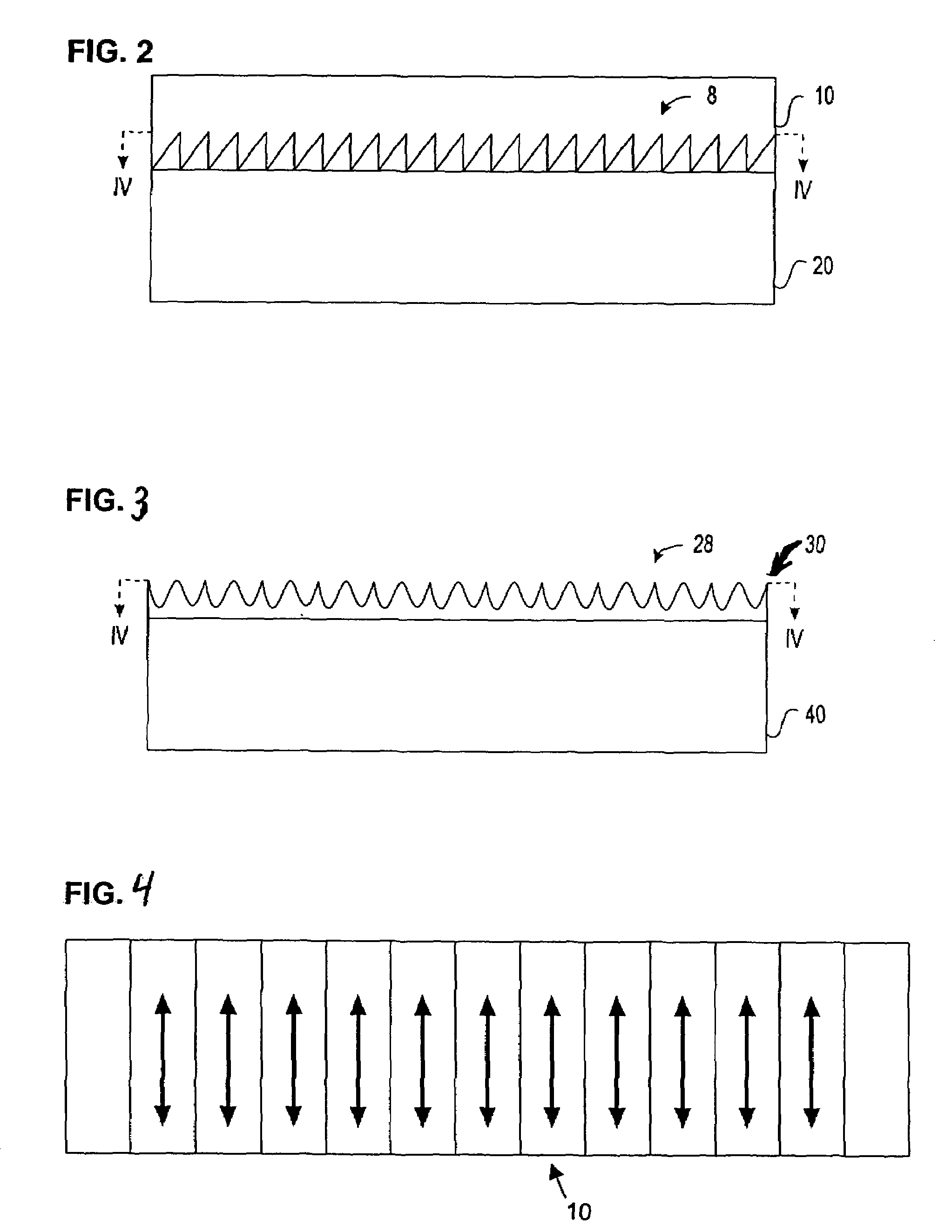
[0021]FIG. 2 shows a partial cross-section of film stack 2 taken along the line II—II in FIG. 1. As illustrated in FIG. 2, seed layer 8 provided above substrate 20 is textured. The texture of the seed layer 8 imparts uniaxial anisotropy in ferromagnetic film 10 grown above seed layer 8. Alignment of the ...


PUM


Abstract

Magneto-resistive random access memory elements include a ferromagnetic layer having uniaxial anisotropy provided by elongate structures formed in the ferromagnetic film. The magnetic dipole aligns with the long axis of each structure. The structures can be formed in a variety of ways. For example, the ferromagnetic film can be applied to a seed layer having a textured surface. Alternatively, the ferromagnetic film can be stressed to generate the textured structure. Chemical mechanical polishing also can be used to generated the structures.

Description

BACKGROUND OF THE INVENTION[0001]1. Field of the Invention[0002]The invention relates to methods of producing magnetoresistive elements, and more particularly, to methods of producing magnetoresistive elements having an induced secondary anisotropy.[0003]2. Description of the Related Art[0004]Storage memories of various types are used extensively in digital systems such as microprocessor-based systems, digital processing systems, and the like. Recently, magnetic random access memory (MRAM) devices have been investigated for possible use in non-volatile random access memory. Information is stored in MRAM devices based on a magnetoresistive effect, in which memory cells formed of ferromagnetic layers in the device have resistances that change based on the magnetized state of a free ferromagnetic layer compared to that of a pinned (fixed) ferromagnetic layer. The magnetic moment of the pinned layer remains fixed while the magnetic moment of the free layer can change depending on an ext...

Claims


Application Information

Patent Timeline
Patent Type & Authority Patents(United States)
IPC IPC(8): H01L21/00G11C11/16H01L27/22H01L43/08H01L43/12
CPCG11C11/16H01L43/12H01L43/08H01L27/222G11C11/161H10B61/00H10N50/10H10N50/01
Inventor DREWES, JOEL A.
Owner MICRON TECH INC
Why Eureka
Try Eureka