Analog delay chain having more uniformly distributed capacitive loads and analog delay cell for use in chain

a capacitive load and analog delay technology, applied in the field of analog delay lines, to achieve the effect of reducing loading capacitance and widening frequency response rang

Inactive Publication Date: 2007-03-13
SCINTERA NETWORKS
View PDF7 Cites 2 Cited by
  • Summary
  • Abstract
  • Description
  • Claims
  • Application Information

AI Technical Summary

Benefits of technology

[0013]A tapped delay chain in accordance with the invention comprises a plurality of delay cells where each cell has at least two output taps: a primary one for feeding forward a delayed signal to a next cell in the chain, and a secondary output tap for feeding a slightly-differently delayed signal to a multiplier unit so that the slightly-differently delayed signal can be multiplied by a weighting coefficient. The split of output taps in each delay cell allows for a corresponding split of loading capacitance. Each output tap of the delay cell is loaded by a smaller capacitance than it would have had to otherwise drive had the split taps been instead lumped together as a common node. The reduced loading capacitance at each of the split taps allows for a wider frequency response range.

Problems solved by technology

A number of problems are associated with FFE's and FS-FFE's.
Another problem is how to simultaneously provide for linear phase shift over the frequency range of interest.
Another problem is how to simultaneously provide for unity gain in each of a series of delay cells while enabling the cells to provide flat magnitude response over the frequency range of interest.

Method used


Image

  • Analog delay chain having more uniformly distributed capacitive loads and analog delay cell for use in chain
  • Analog delay chain having more uniformly distributed capacitive loads and analog delay cell for use in chain
  • Analog delay chain having more uniformly distributed capacitive loads and analog delay cell for use in chain

Examples


Embodiment Construction

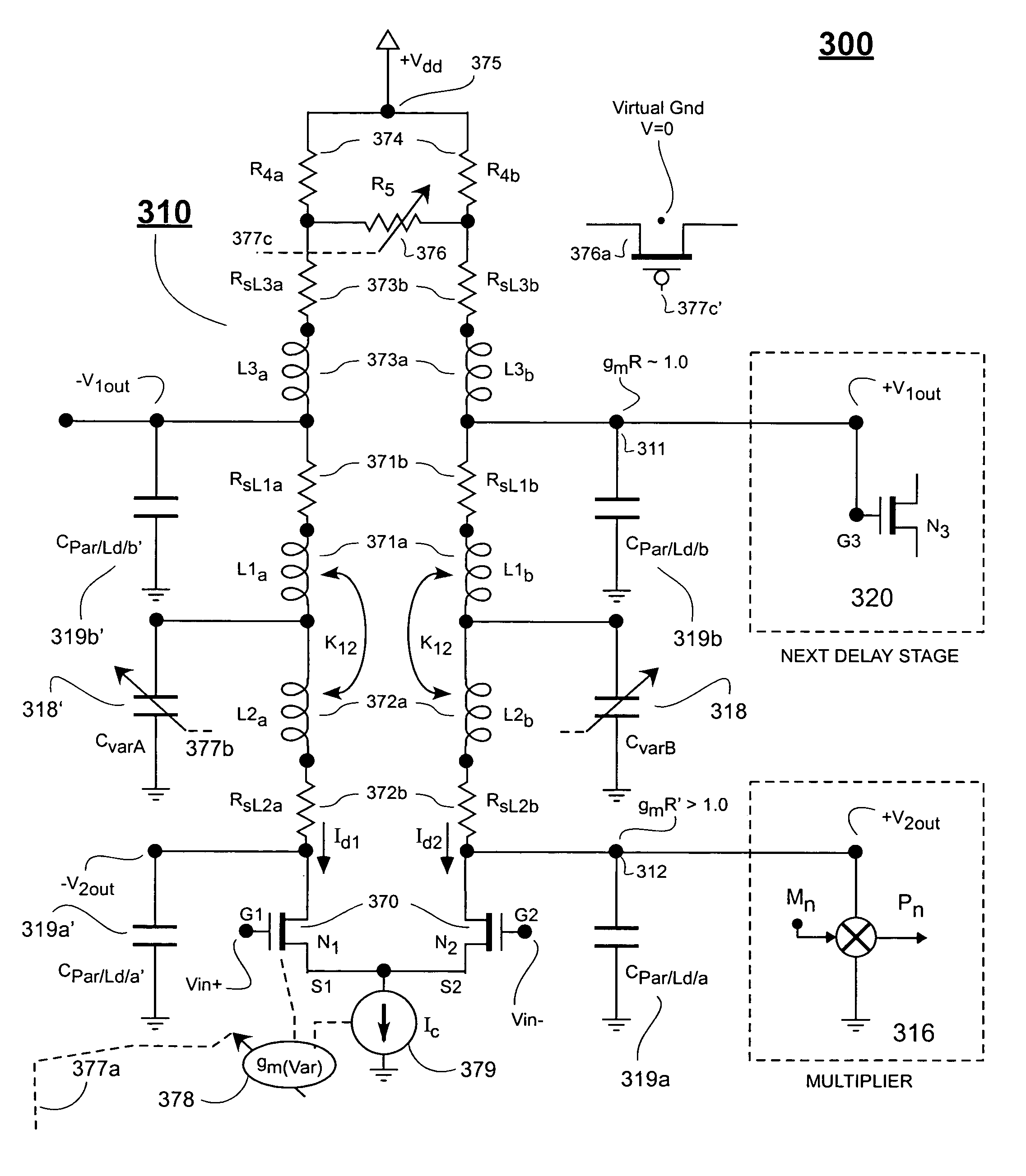
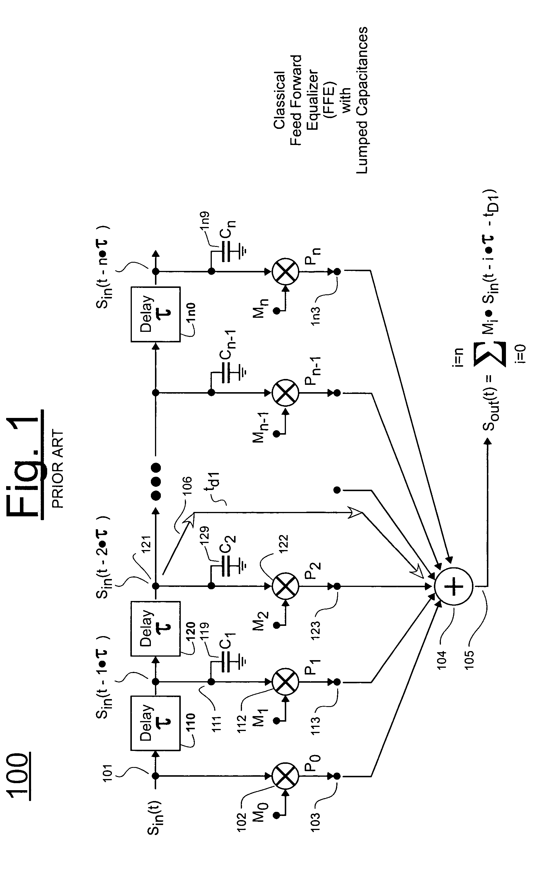
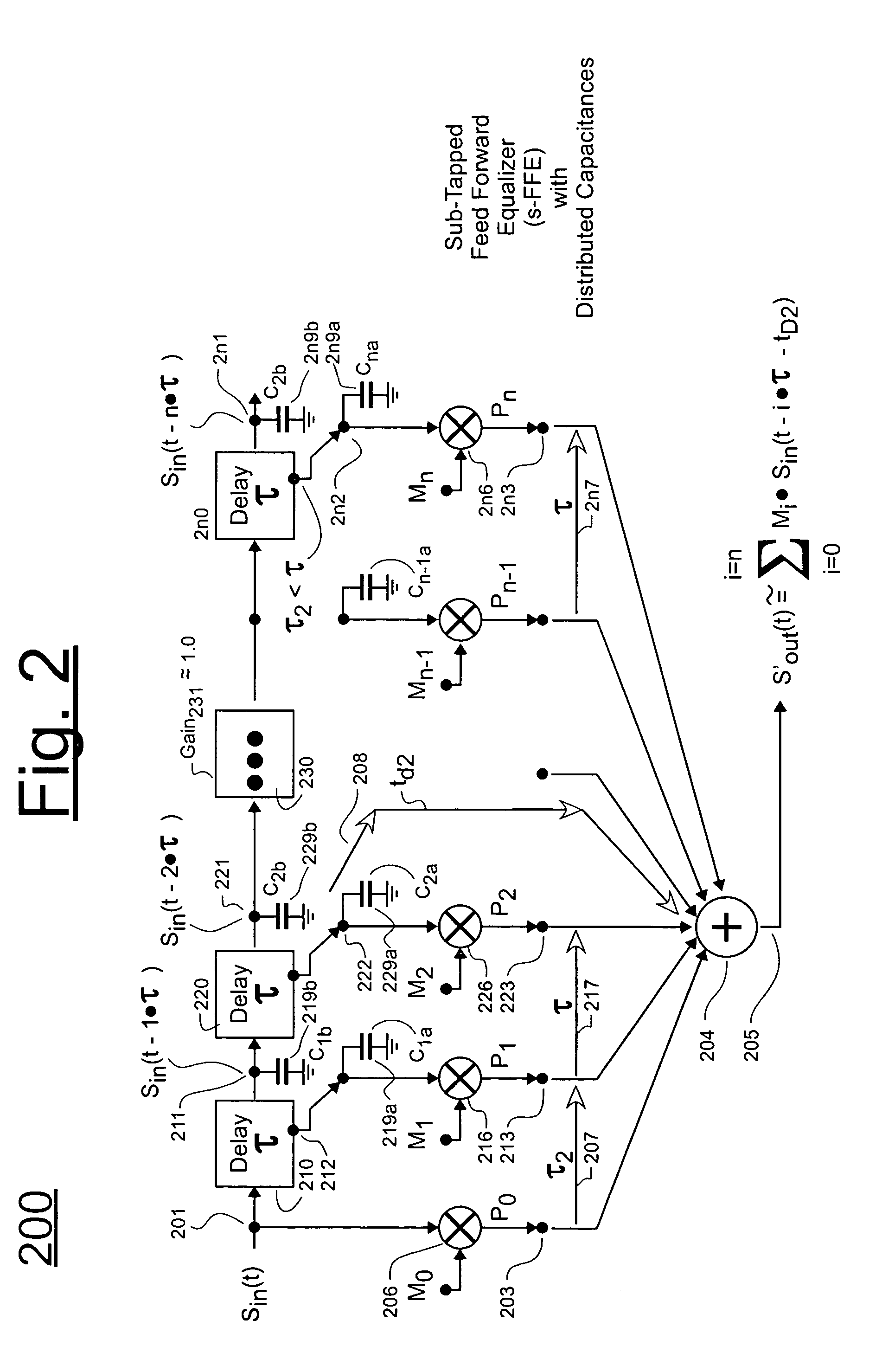
[0023]Referring to FIG. 1, an environment 100 in which cascaded delay cells may be employed is first described. Input signal Sin(t) may be a wide bandwidth communications signal such as that obtained from passing a series of substantially rectangular signal pulses through a transmission medium (e.g., a continuous fiber optic link) that exhibits signal dispersion. To correct for the dispersion, filtering is employed. In one embodiment, periodically delayed versions, Sin(t−i·T / k) of the input signal are generated, where i represents successive ones of a sequential series of whole numbers (0, 1, 2 . . . , n), k is a whole number such as 2 or 3, and τ=T / k, where T is a predefined symbol period. The periodically delayed versions of the input signal are respectively multiplied by independent weighting coefficients (Mi) and the resulting product signals (Pi) are added to produce an adaptively equalized output signal, Sout(t). Adaptive equalization may be carried out by changing the weighti...


PUM


Abstract

A tapped delay chain comprises a plurality of delay cells where each cell has at least two output taps: a primary one for feeding forward a delayed signal to a next cell in the chain, and a secondary output tap for feeding a slightly-differently delayed signal to a multiplier unit so that the slightly-differently delayed signal can be multiplied by a weighting coefficient. The split of output taps in each delay cell allows for a corresponding split of loading capacitance. Each output tap of the delay cell is loaded by a smaller capacitance than it would have had to otherwise drive had the split taps been instead lumped together as a common node. The reduced loading capacitance at each of the split taps allows for a wider frequency response range. The tapped delay chain may be used to form a feed-forward equalizer (FFE) which further comprises an adder, and a plurality of multipliers each respectively receiving a delayed input signal (Sin(delayed)) from a secondary output tap of a respective delay cell in the chain and each outputting a correspondingly delayed and weighted, product signal (Pi) to the adder.

Description

FIELD OF DISCLOSURE[0001]The invention related generally to analog delay line with periodically tapped output nodes and more specifically to high frequency applications in which lumped capacitance can have detrimental effects on response bandwidth. The invention relates yet more specifically to high frequency application where the tapped output nodes of the delay chain are to be utilized, by for example, programmably weighting each and summing them so as define a feedforward equalizer (FFE) or the like.CROSS REFERENCE TO CO-OWNED APPLICATIONS[0002]The following copending U.S. patent applications are owned by the owner of the present application, and their disclosures are incorporated herein by reference:[0003](A) Ser. No. 10 / 724,443 filed: Nov. 26, 2003 by Mukherjee et al and originally entitled “Analog Delay Elements”;[0004](B) Ser. No. 10 / 724,449 filed: Nov. 26, 2003 by Bhattacharjee et al and originally entitled “Digitally Controlled Transconductance Cell”; and[0005](C) Ser. No. ...

Claims


Application Information

Patent Timeline
Patent Type & Authority Patents(United States)
IPC IPC(8): H03F3/45
CPCH03F3/45183H03F2203/45631H03F2203/45712H03F2203/45652H03F2203/45688H03F2203/45638
Inventor MUKHERJEE, DEBANJANBHATTACHARJEE, JISHNU
Owner SCINTERA NETWORKS
Why Eureka
Try Eureka