Display unit and methods of displaying an image

a technology of display unit and image, applied in the field of display unit, can solve the problems of limiting printing methods to those including inks, affecting the visual effect of both sides, and affecting the effect of cos

Inactive Publication Date: 2007-03-20
3M INNOVATIVE PROPERTIES CO
View PDF68 Cites 17 Cited by
  • Summary
  • Abstract
  • Description
  • Claims
  • Application Information

AI Technical Summary

Benefits of technology

[0201]An advantage of the present invention is the ability to eliminate manufacturing steps for the preparation of electrostatic images on a final substrate.
[0202]An electrostatic direct printing film can have a surface resistance in its conductive layer of about 2×10⁵ to about 3×10⁶ Ohms / □ and can have a surface resistance in its dielectric layer of greater than about 1×10⁸ Ohms / □. This difference in surface resistance results in clear, crisp images generated by the electrostatic printer.
[0203]“Surface Resistance” is the measure of D-C resistance of moderately conductive materials according to ASTM Test Designations D 4496-87 and D 257-93.
[0204]Referring to FIG. 13, a typical construction of a film of the present invention 310 comprises a substrate film 312 having on a major surface thereof, a conductive layer 314 and a dielectric layer 316. On the opposite major surface of film substrate 312 resides optional pressure sensitive adhesive 318 protected by a release liner 320.
[0205]For electrostatic imaging on film 310, a conductive coating layer 314 is provided from an organic solvent-based conductive coating solution on the upper major surface of film substrate 312, which can be any substrate described above for prior embodiments. Electronically conductive layers employ a plurality of particles of a transparent, electrically conductive material such as antimony doped tin oxide or the like, disposed in a polymeric matrix. Conductive layer 314 is prepared from a solution of a conductive formulation that generally comprises a binder, conductive pigments, dispersant, and organic-based solvent, the latter which is removed during the manufacturing process. The weight percent of solids to organic solvent in the conductive formulation can range from about 10 to about 40, with about 25 weight percent being presently preferred for ease of application to film substrate 312.
[0206]After coating of conductive formulation on film substrate 312 and evaporation or other removal of organic solvent, the thickness or caliper of the conductive layer 314 can range from about 2 to about 5 μm with about 3 μm being presently preferred.

Problems solved by technology

Vision from either side can be totally or partially obstructed.
The is printing methods are limited to those including inks.

Method used


Image

  • Display unit and methods of displaying an image
  • Display unit and methods of displaying an image
  • Display unit and methods of displaying an image

Examples


first embodiment

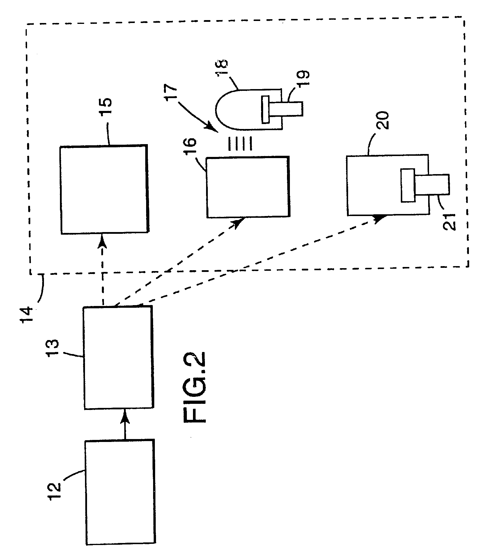
[0068]FIG. 2 shows a schematic block diagram of the present invention. A suitable graphics image for display purposes is generated in image generation means 12. The image may be generated using computer 13 and special software developed for production of graphic images such as Adobe Photoshop™, Adobe Illustrator™, Corel-Draw™, Alduso® Pagemaker™, Quark Xpress™ or similar. The image generation means 12 may be a scanner with which all or part of picture information from an image, a picture or photograph is converted point by point into electrical signals to be stored in computer 13 as digital data.

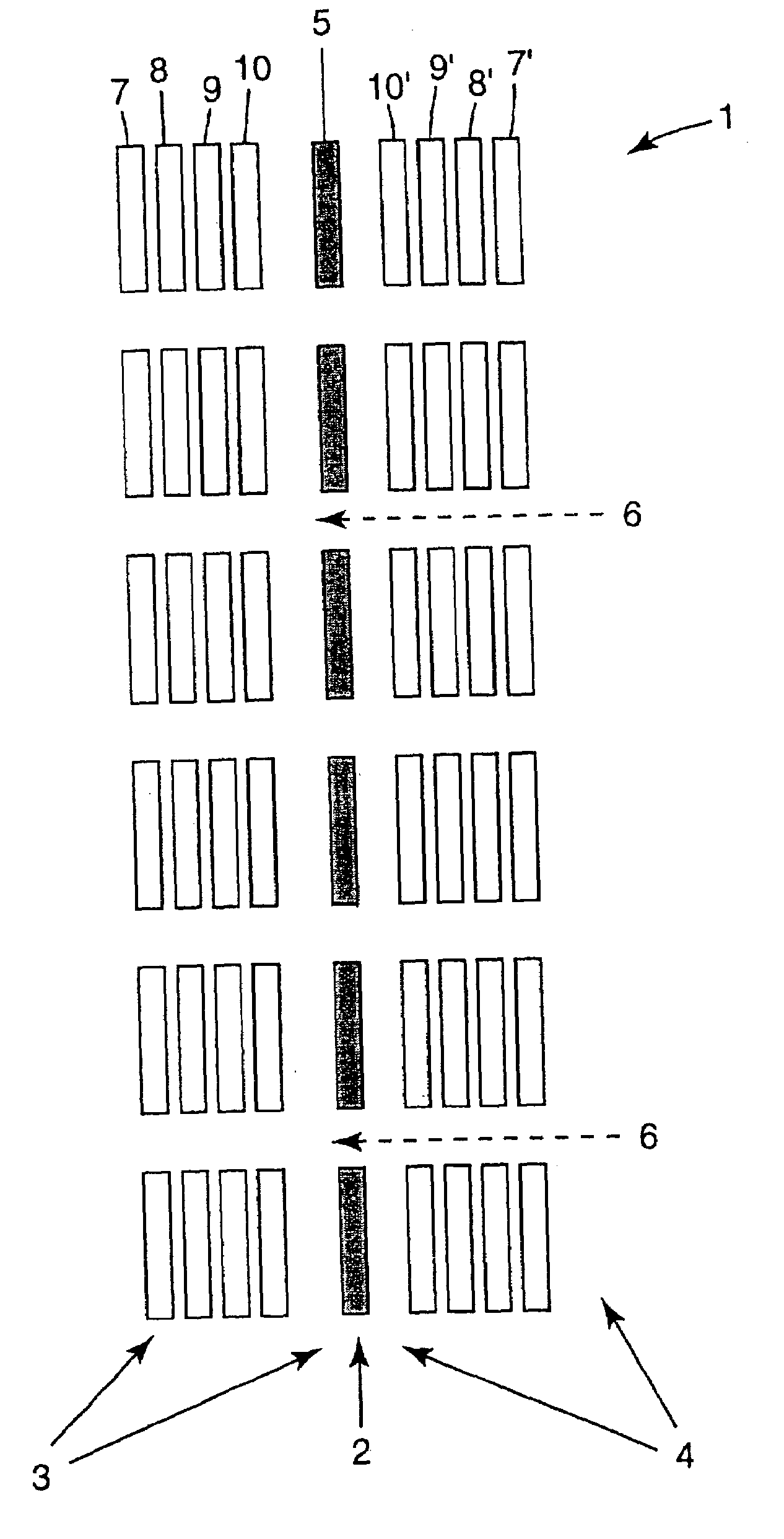
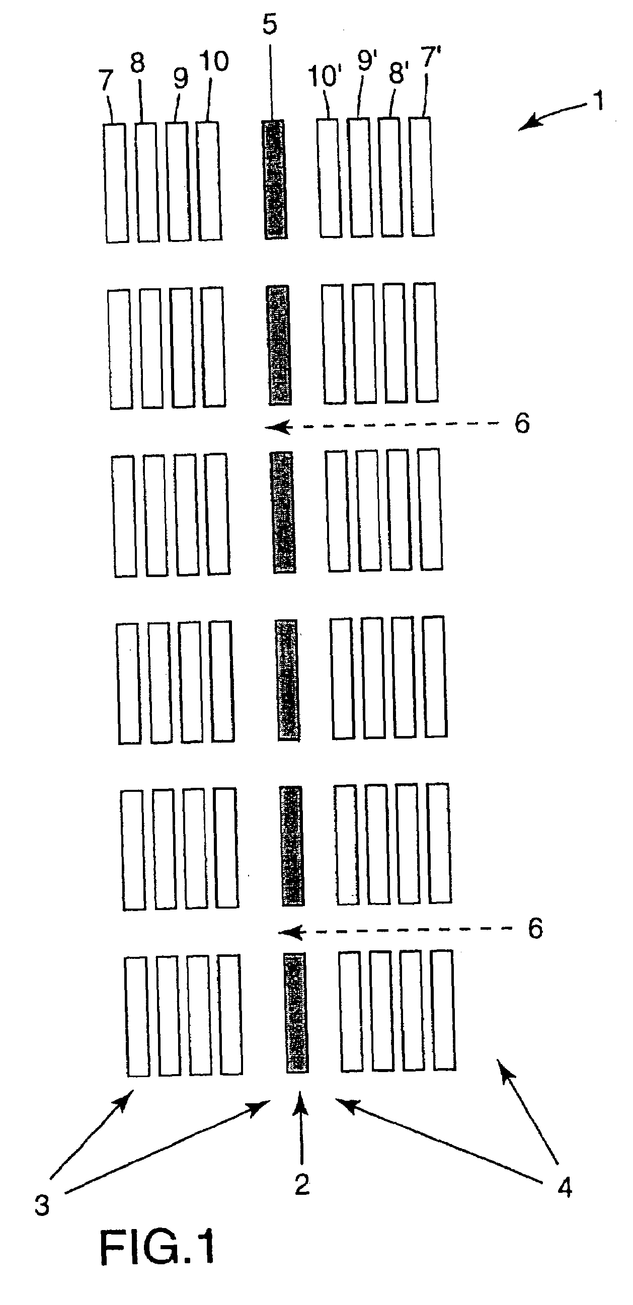
[0069]Once the graphics image has been stored in computer 13 as a matrix of digital data which include sufficient data to determine the luminosity and color of each pixel of information, the data may be prepared such that it may be displayed with a plurality of transparent areas 6 within the graphics image.

[0070]In accordance with the present invention this may be done in several different w...

second embodiment

[0089]A direct or simultaneous display device 15 in accordance with the present invention is a display device which displays at least the image directly from the electrical output of the computer 13 and combines this with the silhouette pattern 2 so that the transparent areas 6 of the silhouette layer 2 are in registry with the transparent areas of the image. Such a direct display device 15 in accordance with the present invention is shown schematically in FIG. 6. A conventional LCD display 24 is addressed by an addressing unit 28 which is connected to the computer 13 in the conventional way e.g. by means of cable and connector 29. The LCD array 24 may form part of a window. Behind the LCD array 24 is placed a back-light or reflector 25 which has a light source 26 connected to a suitable power supply (not shown) by cable and connector 27.

[0090]The back-light 25 produces illumination in the form of strips, squares, circles or similar shapes separated by areas of transparent material ...

third embodiment

[0096]Alternatively, the display device 14 in accordance with the present invention may be an indirect printing device 16–19.

[0097]An indirect printing device in accordance with the present invention is a printing method with which there is sequential colorant transfer of individual color-separated images from intermediate image carriers to the printing substrate. Typically this requires a set of color-separated, i.e. single primary color, intermediate image substrates 17 which are used in printing device 18 to produce the final printed image 19. The intermediate imaged substrates 17 are produced from the computer output data in the intermediate imaging device 16. Such an indirect printing method may be for example lithographic or screen printing.

[0098]With reference to lithographic printing, the imaged substrates 17 may be a series of imaged polyester lithographic plates, suitable for lithographic printing on a printing press 18. The lithographic substrates 17 may be generated dire...


PUM


Abstract

The present invention provides a method of displaying an image on a display device having first and second sides, said image including an light restricting silhouette pattern having a plurality of first transparent or translucent areas, and at least one design layer having at least one color, said at least one design layer being visible from one side of said display device and substantially less visible from the other side, said image being substantially transparent or translucent as viewed from the other side, comprising the steps:1) providing at least a definition of said design layer to a computer;2) generating a computerized version of said design layer with the computer;3) outputting the computerized version of said design layer to said display device, the computerized version of said design layer being modified to subdivide said design layer into a plurality of second discrete transparent or translucent areas and other areas, and4) displaying said modified design layer and said silhouette pattern with said first and second transparent areas being in registry.Articles produced in accordance with the method are also described.Printers, raster image processing methods and systems computer graphics systems are described for producing the article.

Description

CROSS REFERENCE TO RELATED APPLICATIONS[0001]This application is a continuation of U.S. application Ser. No. 10 / 291,067, filed Nov. 8, 2002, now pending, which is divisional of U.S. application Ser No. 09 / 202,281, filed on Dec. 11, 1998, issued as U.S. Pat. No. 6,507,413 on Jan. 14, 2003, which is a 371 of PCT / US96 / 09888, filed Jun. 14, 1996.FIELD OF THE INVENTION[0002]The present invention relates to a display unit, and in particular to a display unit for displaying images viewable from two sides, whereby the image as perceived from one side can be different from the image perceived from the other side and the display unit is transparent or translucent when viewed from one of the sides.[0003]The invention also relates to a method of displaying such an image as well as printers suitable for displaying a printed image and raster image processing (RIP) systems for preparing the data before display, particularly before printing.BACKGROUND OF THE INVENTION[0004]Display devices with diff...

Claims


Application Information

Patent Timeline
Patent Type & Authority Patents(United States)
IPC IPC(8): G06T11/40G06K15/00G09G3/00H04N1/50G06F15/00G06T11/00H04N1/56B44F1/06B41J3/407B41J3/54B44C1/17B44F1/10
CPCB41J3/407B41J3/546B44C1/17B44F1/10G06K15/00G09G5/02Y10T428/24736Y10T428/162Y10T428/24851Y10T428/24876Y10T428/24868Y10T428/24322G06K15/023
Inventor MUELLER, BRUNOBIRD, WILLIAM E.
Owner 3M INNOVATIVE PROPERTIES CO
Why Eureka
Try Eureka