Method and apparatus for full-chip thermal analysis of semiconductor chip designs

a technology of semiconductor chips and thermal analysis, applied in error detection/correction, program control, instruments, etc., can solve problems such as failure of system, failure to provide a complete or entirely accurate picture of the operating thermal gradient of the chip, and failure to solve the temperature in a full three-dimensional dimension

Active Publication Date: 2007-03-20
KEYSIGHT TECH
View PDF4 Cites 33 Cited by
  • Summary
  • Abstract
  • Description
  • Claims
  • Application Information

AI Technical Summary

Problems solved by technology

These semiconductor chips are also often the hottest part of the electronic system, and failure of the system can often be traced back to thermal overload on the chips.
Such conventional methods, however, typically fail to provide a complete or an entirely accurate picture of the chip's operating thermal gradient.
For example, typical thermal analysis models attempt to solve the temperature on the chip substrate, but do not solve the temperature in a full three dimensions, e.g., using industry standards design, package and heat sink data.
Moreover, most typical methods do not account for the sharing of power among semiconductor devices and interconnects, which distributes the heat field within the chip, as discussed above.

Method used


Image

  • Method and apparatus for full-chip thermal analysis of semiconductor chip designs
  • Method and apparatus for full-chip thermal analysis of semiconductor chip designs
  • Method and apparatus for full-chip thermal analysis of semiconductor chip designs

Examples


Embodiment Construction

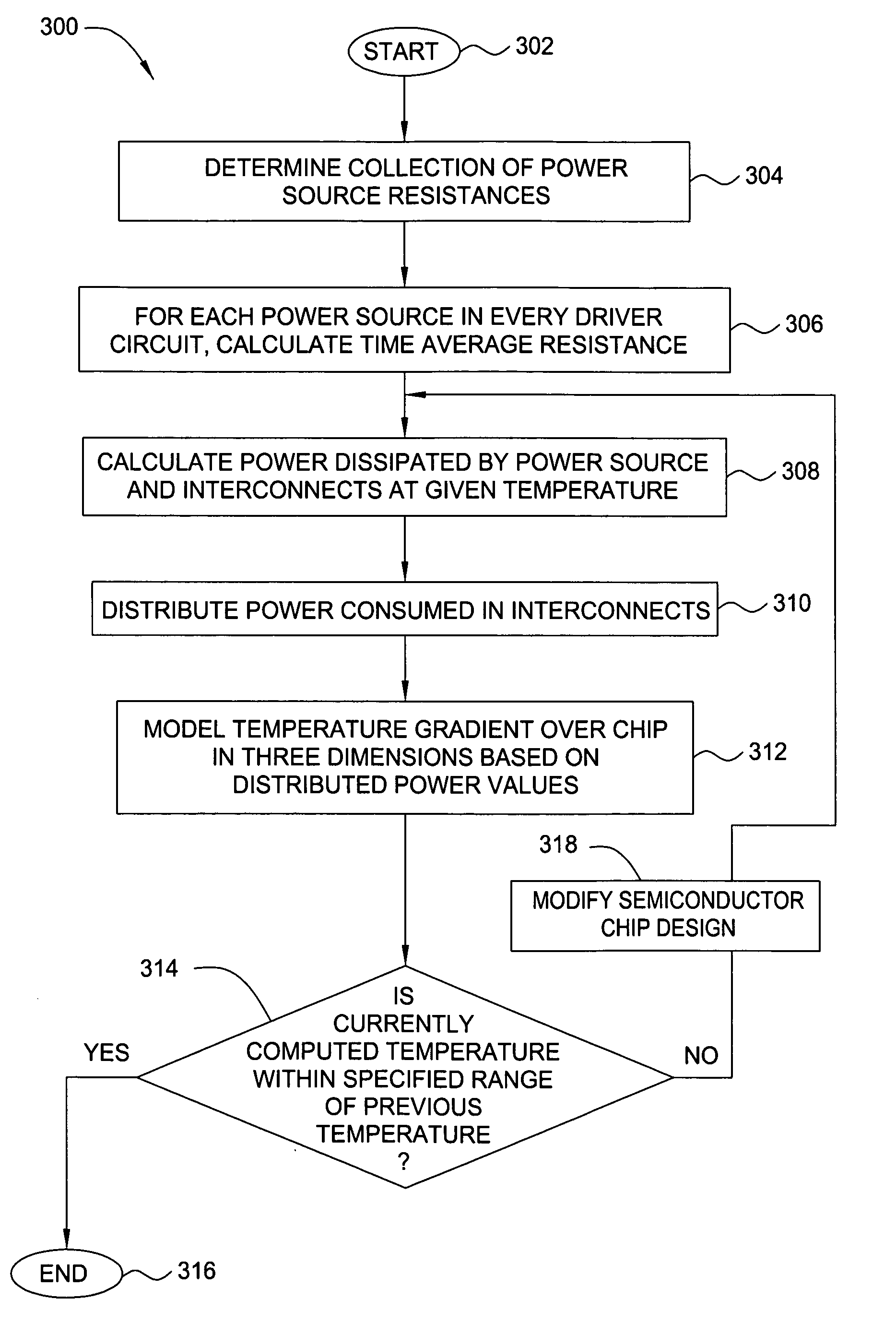
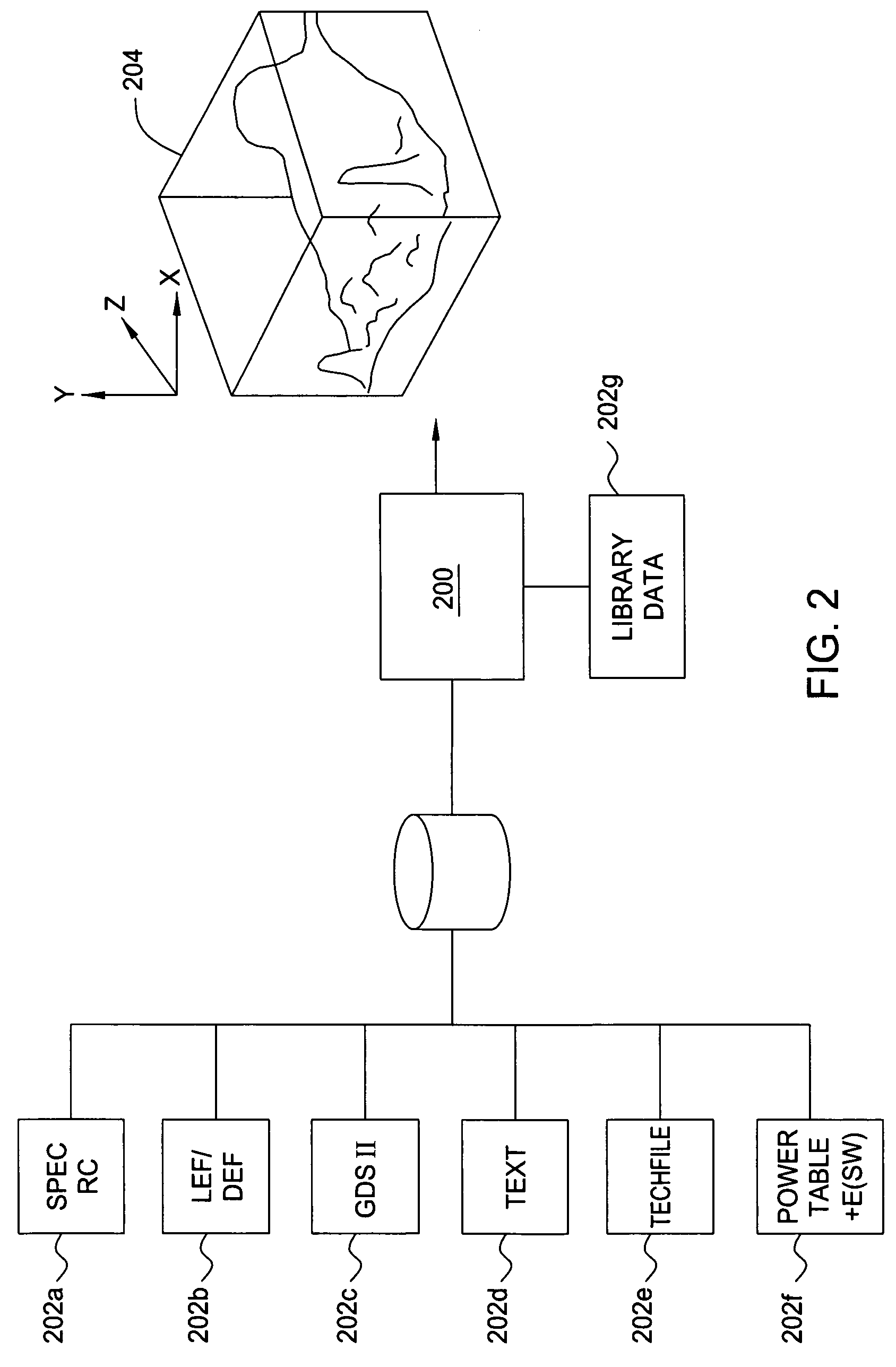
[0015]Embodiments of the invention generally provide a method and apparatus for three-dimensional thermal analysis of semiconductor chip designs. One embodiment of the inventive method produces a full, three-dimensional solution of temperature values within a chip design, including power dissipation values distributed over semiconductor devices (e.g., transistors, resistors, capacitors, diodes and the like) and wire interconnects, thereby providing chip designers with the data necessary to produce more robust semiconductor chips.

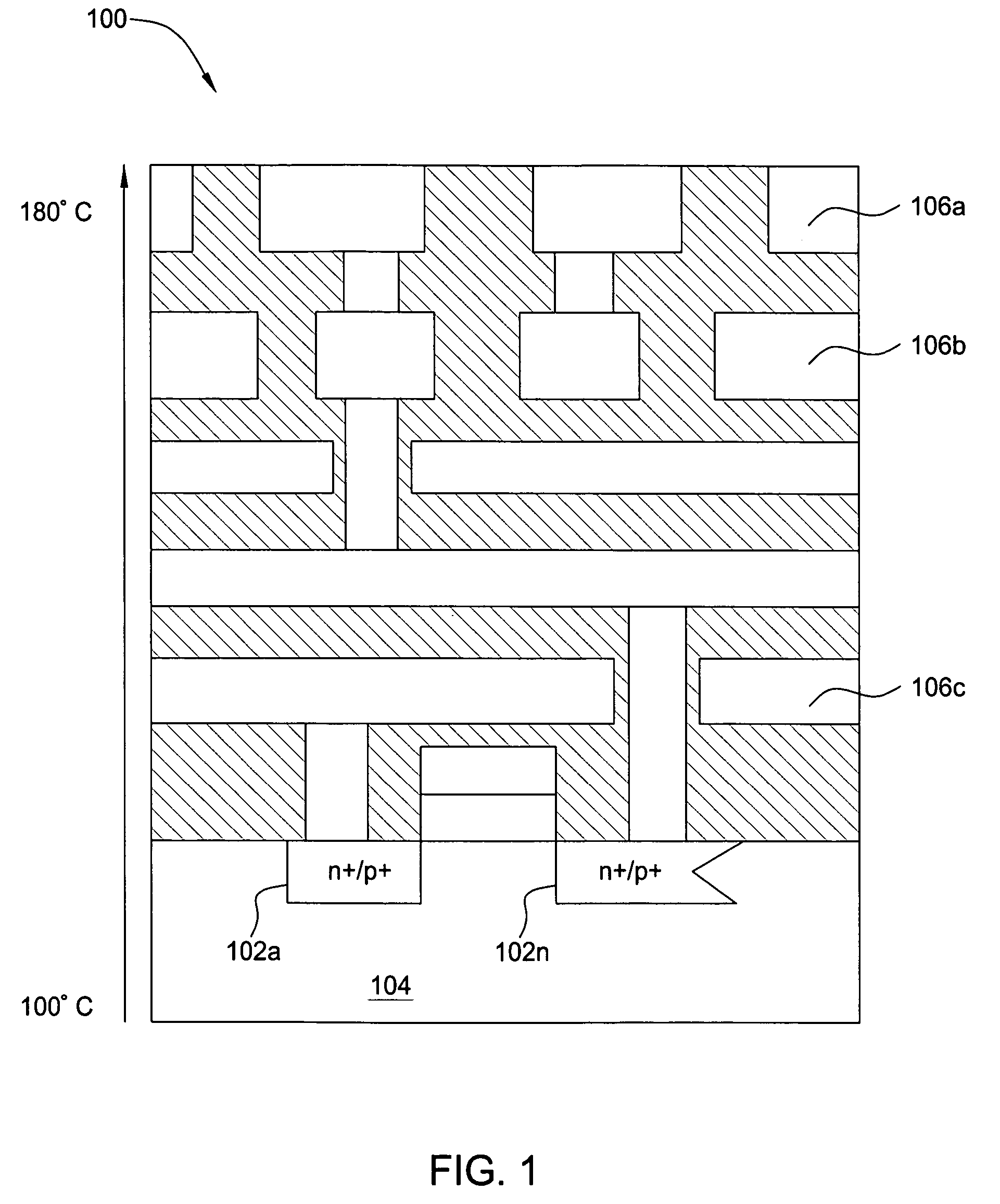
[0016]As used herein, the term “semiconductor chip” refers to any type of semiconductor chip, which might employ analog and / or digital design techniques and which might be fabricated in a variety of fabrication methodologies including, but not limited to, complementary metal-oxide semiconductor (CMOS), bipolar complementary metal-oxide semiconductor (BiCMOS), and gallium arsenide (GaAs) methodologies. Furthermore, as used herein, the term “semiconductor devi...


PUM


Abstract

A method and apparatus for full-chip thermal analysis of semiconductor chip designs is provided. One embodiment of a novel method for performing thermal analysis of a semiconductor chip design comprises receiving at least one input relating to a semiconductor chip design to be analyzed. The input is then processed to produce a three-dimensional thermal model of the semiconductor chip design. In another embodiment, thermal analysis of the semiconductor chip design is performed by calculating power dissipated by transistors and interconnects included in the semiconductor chip design and distributing power dissipated by the interconnects.

Description

CROSS REFERENCE TO RELATED APPLICATIONS[0001]This application claims the benefit of U.S. Provisional Patent Application Ser. No. 60 / 539,727, filed Jan. 28, 2004 (entitled “Method and Apparatus for Improving Constant Temperature Based Timing Analysis of Integrated Circuits By Using Computed Thermal Gradients”), which is herein incorporated by reference in its entirety.FIELD OF THE INVENTION[0002]The present invention generally relates to semiconductor chip design, and more particularly relates to the thermal analysis of semiconductor chip designs.BACKGROUND OF THE INVENTION[0003]Semiconductor chips typically comprise the bulk of the components in an electronic system. These semiconductor chips are also often the hottest part of the electronic system, and failure of the system can often be traced back to thermal overload on the chips. As such, thermal management is a critical parameter of semiconductor chip design.[0004]FIG. 1 is a schematic diagram illustrating an exemplary semicondu...

Claims


Application Information

Patent Timeline
Patent Type & Authority Patents(United States)
IPC IPC(8): G06F17/50
CPCG06F17/5036G06F30/367
Inventor CHANDRA, RAJIT
Owner KEYSIGHT TECH
Why Eureka
Try Eureka