Emissive flat panel display having electron sources with high current density and low electric field strength

a flat panel display and electron source technology, applied in the field of display devices, can solve the problems of coarse display screen and non-uniform display, and achieve the effect of increasing the emission site density

Inactive Publication Date: 2007-03-27
HITACHI DISPLAYS
View PDF3 Cites 82 Cited by
  • Summary
  • Abstract
  • Description
  • Claims
  • Application Information

AI Technical Summary

Benefits of technology

[0010]Accordingly, it is the first object of the present invention to provide an emissive flat panel display device which can perform the gate operation at a relatively low voltage of several V to several tens V using gate electrodes.
[0012]It is the second object of the present invention to provide an emissive flat panel display device which can realize uniform display images having no coarseness by setting the density of the emission site which constitutes electron sources to one million pieces / cm2 or more and preferably to ten-million pieces / cm2 or more.
[0014]Further, according to the present invention, by setting the maximum emission current density to 10 mA / cm2, and preferably 30 mA / cm2, it is possible to make the emission current density and the electric field strength of all pixels in the display region satisfy the above-mentioned relationship.
[0015]Further, to achieve the above-mentioned second object, the present invention adopts nanotubes having the narrow diameter distribution as electron sources so as to increase the emission site density. Particularly, by setting the average density of nanotubes having the diameter in which the diameter ranges from the minimum diameter to the maximum diameter which is 1.2 times, and preferably 1.1 times as large as the minimum diameter to ten million pieces / cm2 or more, it is possible to increase the emission site density to one million pieces / cm2 or more, preferably ten million pieces / cm2 or more.

Problems solved by technology

Further, conventionally, since the density of the emission site is extremely low, that is, several thousands pieces / cm2, the display screen appears coarse thus providing a non-uniform display.

Method used


Image

  • Emissive flat panel display having electron sources with high current density and low electric field strength
  • Emissive flat panel display having electron sources with high current density and low electric field strength
  • Emissive flat panel display having electron sources with high current density and low electric field strength

Examples


first embodiment

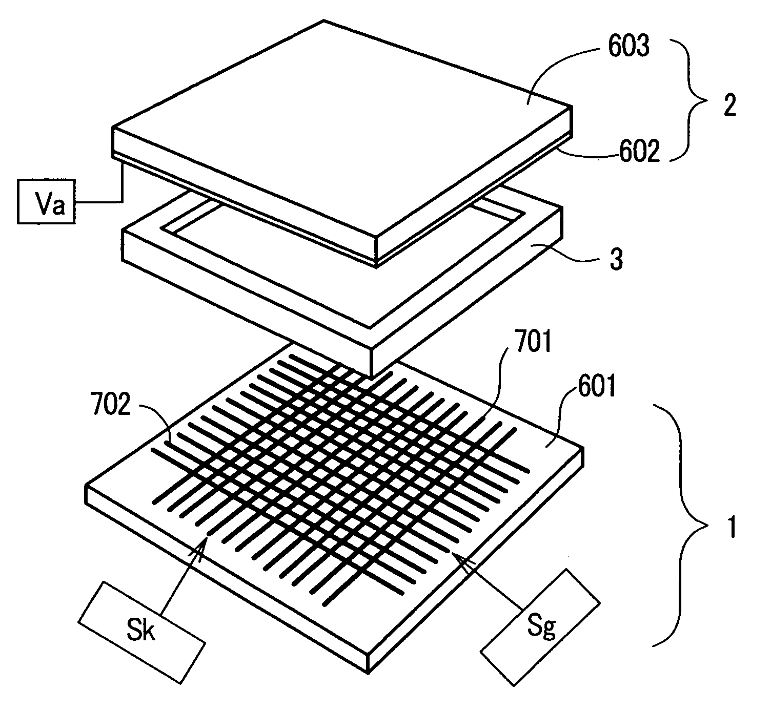
[0065]Next, the detailed structure of the back panel is explained in conjunction with FIG. 15 to FIG. 17. FIG. 15 is a plan view for schematically explaining the structure of an essential part of the back panel and shows a portion where the pixels are provided in a 2×2 array. FIG. 16 is a cross-sectional view taken along a line A–A′ in FIG. 15 and FIG. 17 is a cross-sectional view taken along a line B–B′ in FIG. 15. In FIG. 15 to FIG. 17, on a surface of the back substrate 909 (corresponding to reference numeral 601 in FIG. 11 and FIG. 12) made of glass, 600 stripe-like cathode electrodes 901 (corresponding to reference numeral 701 in FIG. 11 and FIG. 12) having a thickness of 0.2 to 10 μm and a width of 300 μm are formed at an interval of 60 μm. Next, an insulation layer 905 is formed in a state that the insulation layer 905 covers the cathode electrodes 901. A thickness of the insulation layer 905 is set to 1 to 50 μm. In the pixel portion of the insulation layer, that is, in the ...

second embodiment

[0075]Next, the detailed structure of the back panel is explained in conjunction with FIG. 22 to FIG. 24. FIG. 22 is a plan view for schematically explaining the structure of an essential part of the back panel of the emissive flat panel display device of the present invention and shows a portion where the pixels are provided in a 2×2 array. FIG. 23 is a cross-sectional view taken along a line A–A′ in FIG. 22 and FIG. 24 is a cross-sectional view taken along a line B–B′ in FIG. 22. In FIG. 22 to FIG. 24, on a surface of the back substrate 1109 (corresponding to reference numeral 601 in FIG. 11 and FIG. 12) preferably made of glass, 600 cathode electrodes 1101 (corresponding to reference numeral 901 in FIG. 15 to FIG. 17) having a thickness of 0.2 to 10 μm and a width of 300 μm are formed at an interval of 60 μm. Next, an insulation layer 1105 is formed in a state that the insulation layer 1105 (corresponding to reference numeral 905 in FIG. 15 to FIG. 17) covers the cathode electrod...


PUM


Abstract

The present invention provides an emissive flat panel display device which is capable of performing a gate operation at a relatively low voltage of several V to several tens V using gate electrodes. In the emissive flat panel display device which includes a back panel which is constituted of a back substrate on which cathode electrodes having electron sources formed of carbon nanotubes and gate electrodes are formed, a face panel which forms phosphors and anode electrodes thereon, and a sealing frame which seals the back panel and the face panel, the difference between an electric field strength Emax for allowing the electron sources to obtain the required maximum emission current density and an electric field strength Emin which becomes the minimum emission current density is set to 1V / μm or less, and preferably 0.5V / μm or less.

Description

BACKGROUND OF THE INVENTION[0001]The present invention relates to a display device which utilizes an emission of electrons into a vacuum, and more particularly, to an emissive flat panel display device including a back panel which is provided with cathode electrodes having electron sources formed of nanotube and gate electrodes which control an emission quantity of electrons from the electron sources and a face panel which is provided with phosphor layers of plurality of colors which emit light upon excitation of electrons taken out from the back panel and anode electrodes.[0002]As a display device which exhibits the high brightness and the high definition, color cathode ray tubes have been popularly used conventionally. However, along with the recent request for the higher quality of images of information processing equipment or television broadcasting, the demand for planar display devices which are light in weight and require a small space while exhibiting the high brightness and...

Claims


Application Information

Patent Timeline
Patent Type & Authority Patents(United States)
IPC IPC(8): H01J1/62H01J1/00H01J1/30H01J29/04H01J1/304H01J31/12H01J63/04
CPCB82Y10/00H01J1/304H01J31/127H01J29/04H01J2201/30469
Inventor OKAI, MAKOTOMUNEYOSHI, TAKAHIKOYAGUCHI, TOMIOHAYASHI, NOBUAKI
Owner HITACHI DISPLAYS
Why Eureka
Try Eureka