Semiconductor laser device and method of fabricating the same

a laser device and semiconductor technology, applied in the field of semiconductor laser devices, can solve the problems of difficult device implementation, difficult regrowth, fragile physical impact of conventional rwg laser devices b>10/b>, etc., and achieve the effect of stable physical impact and single transverse mod

Active Publication Date: 2007-03-27
SAMSUNG ELECTRONICS CO LTD
View PDF5 Cites 7 Cited by
  • Summary
  • Abstract
  • Description
  • Claims
  • Application Information

AI Technical Summary

Benefits of technology

[0015]According to a second aspect of the present invention, there is provided a semiconductor laser device that includes a semiconductor substrate having a first surface and a second surface that are opposite to one another, and, in order, a first conductive type clad, an active layer, an etch stop layer, a current blocking layer formed in a V-groove shape so that a part of the etch stop layer is exposed, a second conductive type clad formed over the entire of the V-groove and the current blocking layer, an optical guide layer, a current pass facilitation layer, a cap layer, a second conductive type electrode, a first conductive type electrode formed on the second surface of the semiconductor substrate, and first and second trenches formed at right and left sides of the V-groove by etching from the cap layer to the first conductive type clad. It can also increase frequency bandwidth of device reducing parasitic capacitance.

Problems solved by technology

However, because AlGaInAs based materials contain aluminum, oxidation film is naturally formed when the AlGaInAs based materials are exposed to the air; therefore, re-growth is not easy, and thus it is difficult to implement a device.
However, such a conventional RWG laser device 10 is fragile to physical impact, because the ridge 16 is projected.
Furthermore, it is very difficult to form an ohmic contact layer on a mesa whose size is a few micrometers.
In addition, such a projected ridge may be the cause of increasing chip resistance.
In so doing, however, optical guiding becomes too intensive in trenches 17, thereby deteriorating a mode characteristic and causing a kink.
Implementing an optical communication device of high quality is problematic, due to limits on mesa width and space layer thickness reduction for the conventional RWG type laser device.
With the BR type laser device 20, it is difficult to fabricate the ridge in a reversed trapezoid form due to re-growth of the current blocking layer 25.
Because the ridge is widened just above the active layer 22, electric current is not collected on one side but spread out, the unavoidable result of which is an unstable mode characteristic.

Method used


Image

  • Semiconductor laser device and method of fabricating the same
  • Semiconductor laser device and method of fabricating the same
  • Semiconductor laser device and method of fabricating the same

Examples


Embodiment Construction

[0023]Preferred embodiments of the present invention are described with reference to the accompanying drawing. Details of known functions and configurations incorporated herein are omitted for clarity of presentation.

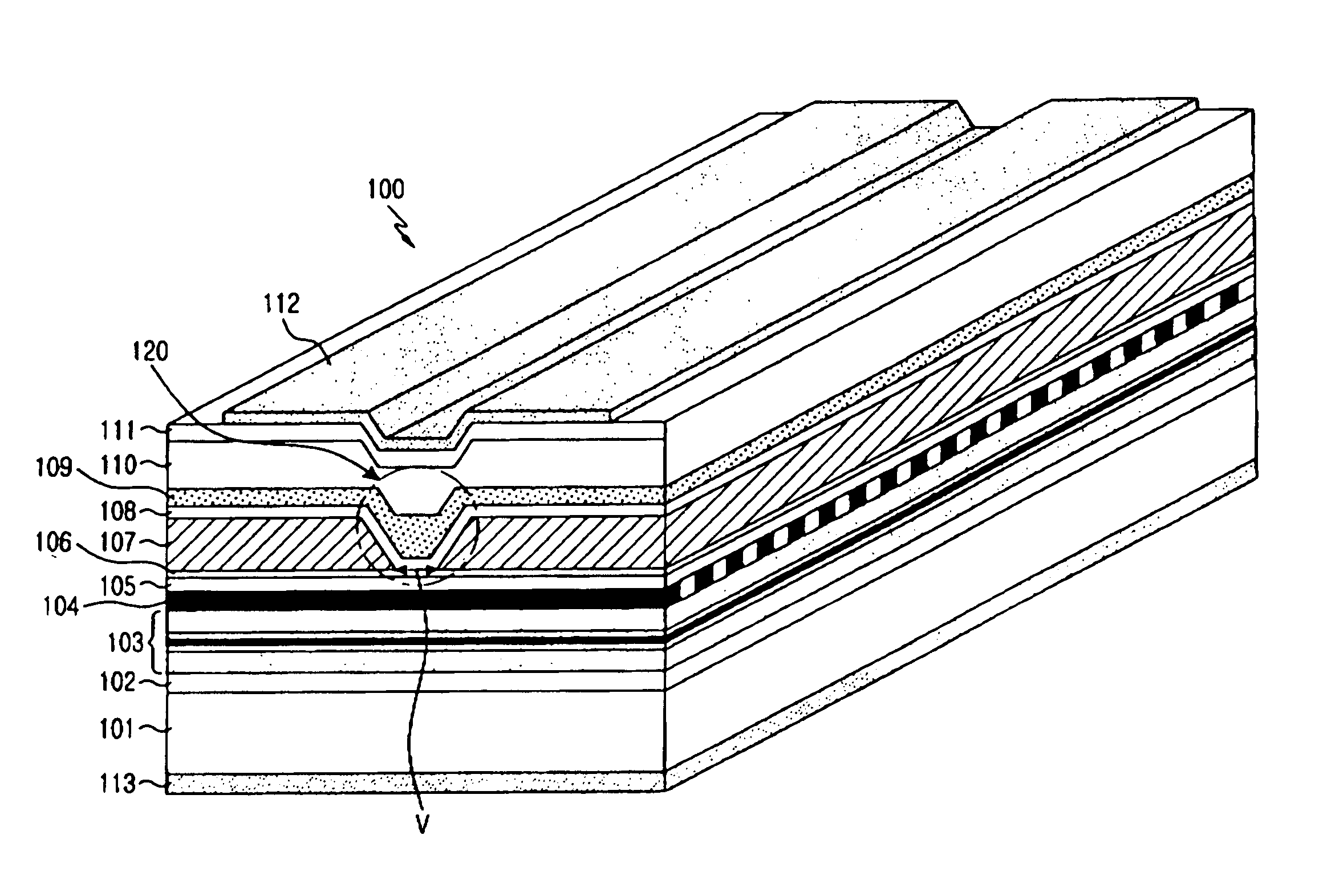
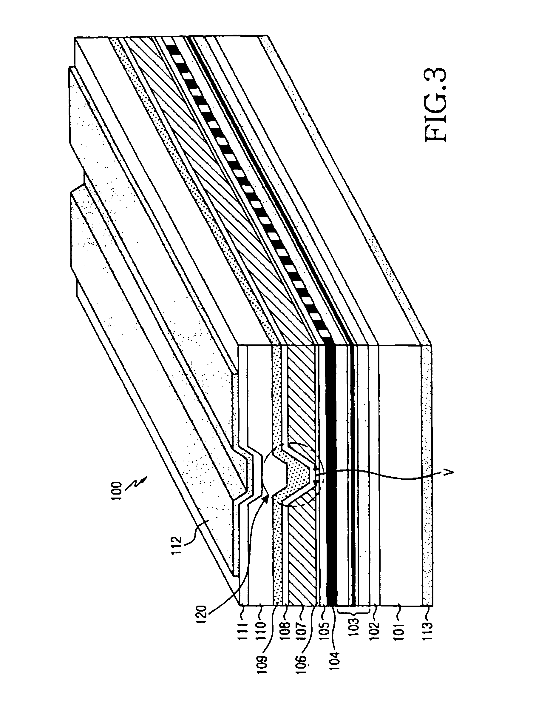
[0024]FIG. 3 is a perspective view showing, by way of illustrative and non-limitative example, a semiconductor laser device 100 according to an embodiment of the present invention. The semiconductor laser device 100 is formed in such a manner that an n-InP clad 102, an AlGaInAs MQW active layer 103, a grating 104, a p-InP space layer 105, and an etch stop layer 106 are sequentially laminated on an n-InP substrate 101, and then a current blocking layer (CBL) 107 is formed on the etch stop layer to have a V-groove shape. Then, a p-InP clad 108, a p-InGaAsP optical guide layer 109, a p-InP current pass facilitation layer 110, a p-InGaAs cap layer 111, and a p-electrode 112 are formed over the current blocking layer 107 and the V-groove region 120, and an n-electrode 113 is...


PUM


Abstract

The width of a current pass region of a semiconductor laser device is narrowed as much as possible, thus implementing a stable single transverse mode. The device is relatively resistant against physical impact. The device includes a semiconductor substrate having first and second opposite surfaces, and, in order, a first conductive type clad, active layer, etch stop layer, current blocking layer formed in a V-groove shape so that a part of the etch stop layer is exposed, second conductive type clad formed entirely over the entire of the V-groove and the current blocking layer, optical guide layer, current pass facilitation layer, cap layer, second conductive type electrode, and a first conductive type electrode formed on the second surface of the semiconductor substrate.

Description

CLAIM OF PRIORITY[0001]This application claims priority to an application entitled “Semiconductor Laser Device and Method of Fabricating the Same,” filed with the Korean Intellectual Property Office on Jan. 8, 2004 and assigned Serial No. 2004-1204, the contents of which are hereby incorporated by reference.BACKGROUND OF THE INVENTION[0002]1. Field of the Invention[0003]The present invention relates to a semiconductor laser device and method of fabricating the same, and, in particular to a device in which a width of a current pass region is controlled in the device, thereby stabilizing a single transverse mode.[0004]2. Description of the Related Art[0005]Four-element systems, as such as InGaAsP, AlGaInAs, etc., are commonly in use as InP-based semiconductor compounds for optical communication semiconductor lasers, and recently, AlGaInAs based materials have become spotlighted to a great extent, as a result of rising demand for greater high-temperature properties and high-speed modul...

Claims


Application Information

Patent Timeline
Patent Type & Authority Patents(United States)
IPC IPC(8): H01S5/24H01S5/223H01S5/00H01S5/12H01S5/22H01S5/323H01S5/343
CPCB82Y20/00H01S5/2202H01S5/12H01S5/34366B60P3/035B60P1/64B60Y2200/147
Inventor HWANG, SUN-LYEONG
Owner SAMSUNG ELECTRONICS CO LTD
Why Eureka
Try Eureka