Lighting emitting device and electronic apparatus having the same

a technology of light emitting device and electronic apparatus, which is applied in the direction of static indicating device, discharge tube luminescnet screen, instruments, etc., can solve the problems of reducing light-emission efficiency, and achieve the effect of increasing the added value of portable digital assistants, versatile and convenient us

Inactive Publication Date: 2007-04-03
SEMICON ENERGY LAB CO LTD
View PDF49 Cites 95 Cited by
  • Summary
  • Abstract
  • Description
  • Claims
  • Application Information

AI Technical Summary

Benefits of technology

[0025]According to the present invention, a thin lightweight light emitting device capable of double-sided display can be provided.
[0026]Particularly, conventionally, on a connection with space or cost a large subscreen can be mounted to portable digital assistants which could mount only a small subscreen, thus increasing the added value of portable digital assistants.
[0027]Mounting the display unit according to the present invention to electronic books and notebook computers allows versatile and convenient use.

Problems solved by technology

When a display having the organic EL elements with such a structure as pixel is displayed by active matrix driving, TFTs on the substrate block off the light that has passed through the anode, significantly reducing light-emission efficiency.

Method used


Image

  • Lighting emitting device and electronic apparatus having the same
  • Lighting emitting device and electronic apparatus having the same
  • Lighting emitting device and electronic apparatus having the same

Examples


embodiment mode 1

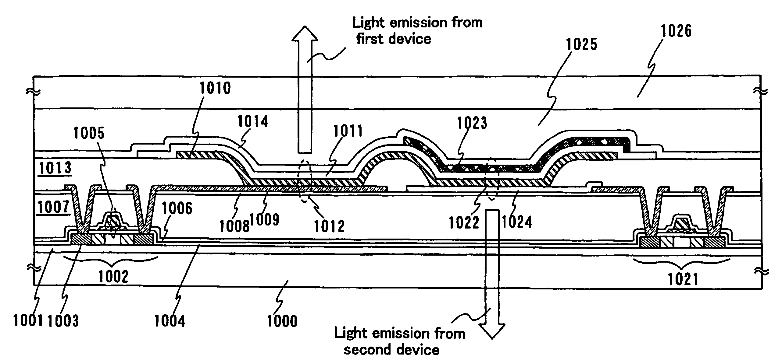
[0041]The structure of pixels and sealing and a method for manufacturing the same according to the present invention will be described herein below. The principal structure of the pixels of the present invention is shown in FIG. 1. Although an active matrix driving TFT is shown here, the driving system may be a simple matrix system.

[0042]The principal structure of the light emitting device of the invention is roughly classified into a first substrate, a first light emitting element and a TFT for driving it, a second light emitting element and a TFT for driving it, a transparent protective film, a sealing agent, and a second substrate. The first light emitting element emits light perpendicular to the surface of the substrate and only in a direction from the side of the substrate to the side having the pixel portion by using a first anode 1009 as reflecting electrode and a cathode 1011 as transparent electrode. The second light emitting element emits light perpendicular to the surface...

embodiment mode 2

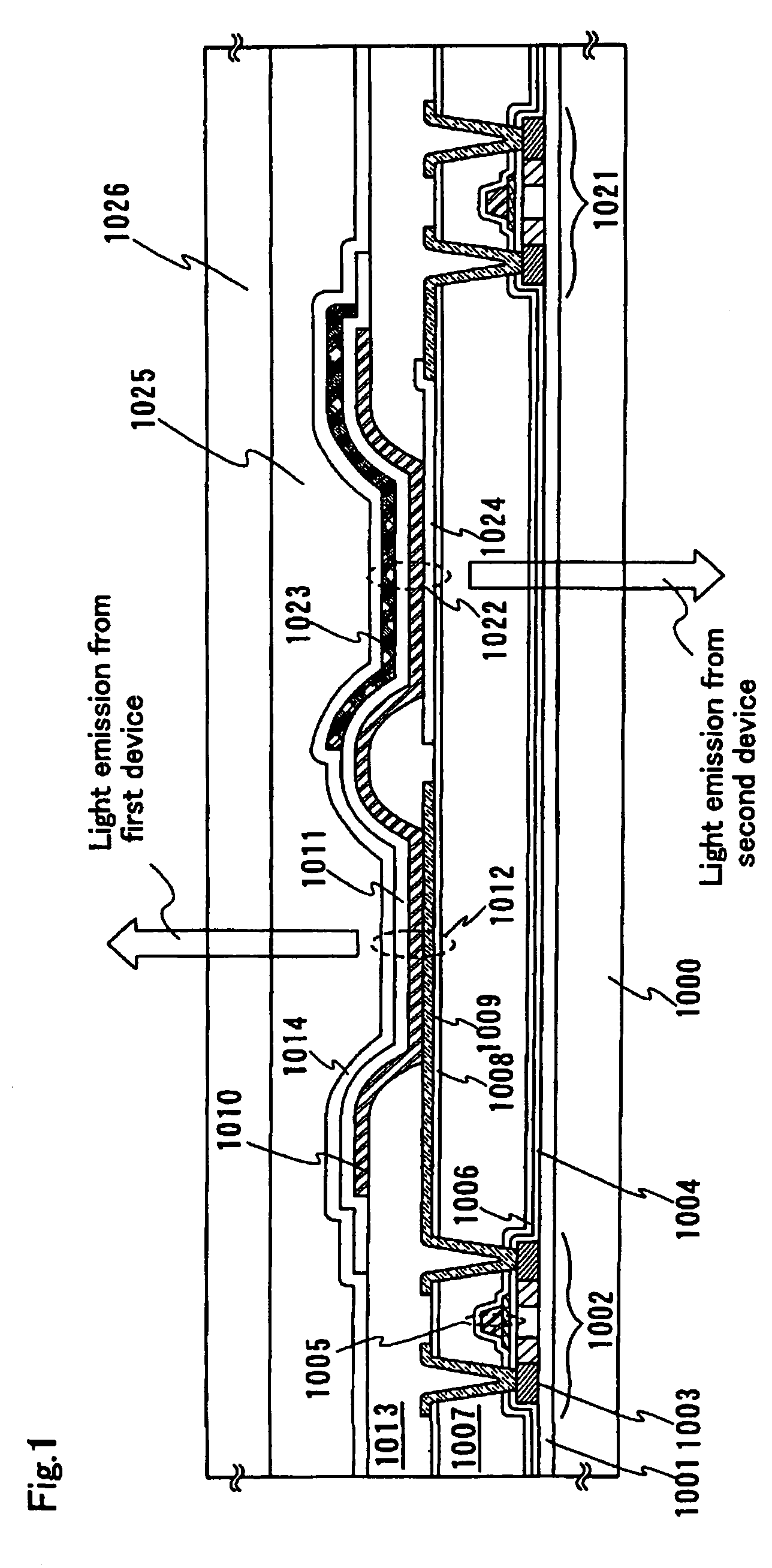
[0065]FIG. 11 shows the principal structure of the pixels of the present invention. Here the structure of a simple matrix light emitting device is shown. In this embodiment, the same components as those of the embodiment mode 1 are described with reference to the same numerals.

[0066]The light emitting device according to the embodiment is constructed such that the first light emitting element 1012 and the second light emitting element 1022 are provided between the first substrate 1000 and the second substrate 1026, and the substrates are fixed together with a space therebetween with an adhesive 1033 containing spacers. An anode 1031 and the positive 1011 are transparent electrodes. The first light emitting element 1012 has a light-shielding film 1030 on the side of the anode 1031, while the second light emitting element 1022 has a light-shielding film 1032 on the side of the cathode 1011, respectively, thereby setting the direction of emitting light.

[0067]In the simple matrix system...

embodiment mode 3

[0074]A method for driving the light emitting device according to the embodiment mode 1 of the invention will now be described with reference to the following embodiment mode 3.

[0075]An embodiment of the invention is shown in FIG. 3. Although thin-film transistors TFTs) are used here as switching elements and driving elements, they are not particularly limited to those. For example, MOS transistors, organic transistors, molecular transistors, etc. may be used similarly. Since the TFTs cannot be classified between a source region and a drain region depending on the structure and their operating conditions, one is expressed as a first electrode and the other as a second electrode.

[0076]Referring to FIG. 3, the region surrounded by a dotted-line frame 3000 forms one pixel and has a source signal line 3001, a gate signal line 3002, a current supply line 3003, a switching TFT 3004, a first driving TFT 3005, a second driving TFT 3006, a first light emitting element 3007, and a second ligh...


PUM


Abstract

One pixel is divided into a first region including a first light emitting element and a second region including a second light emitting element, wherein the first region emits light in one direction and the second region emits light in the direction opposite to that of the first region. Independently driving the first light emitting element and the second light emitting element allows images to be displayed independently on the surface.

Description

TECHNICAL FIELD[0001]The present invention relates to a light emitting device including a pixel portion including light emitting elements having a light emitting layer containing an electro luminescence (EL) material between a pair of electrodes.BACKGROUND ART[0002]Research on light emitting devices using an EL device as spontaneous light emitting element has been actively done. Such light emitting devices are also referred to as organic EL displays or organic light emitting diodes. Because of its features of high response speed, low voltage, and low-power-consumption drive suitable for displaying moving images, the light emitting devices attract considerable attention as next-generation displays including new-generation cellular phones and personal digital assistants (PDA).[0003]EL devices using organic compound layers as light emitting layers have a structure in which a multilayer film is deposited on a substrate, the multilayer film including at least one layer made of an EL mate...

Claims


Application Information

Patent Timeline
Patent Type & Authority Patents(United States)
IPC IPC(8): H01J1/70H01L27/32H01L51/00H01L51/40H01L51/52H05B33/10H05B33/14
CPCH01L27/3267H01L51/5237H01L51/0011Y10T428/24942H01L51/5262H01L2251/558H01L2924/0002H10K59/128H10K71/166H10K50/85H10K50/8426H10K50/844H10K2102/351H01L2924/00H01L33/08H01L33/44H01L33/60H01L33/502H01L27/156H01L25/0753H01L31/0232H10K59/127H10K50/11H10K50/84H10K59/122G06F1/1637G09G3/3225G09G2300/08G09G2320/0626G09G2380/14
Inventor FUJII, TERUYUKIYAMAZAKI, SHUNPEI
Owner SEMICON ENERGY LAB CO LTD
Why Eureka
Try Eureka