Liquid crystal display

a liquid crystal display and display technology, applied in the field of liquid crystal display, can solve the problems of inability to solve second problem, insufficient charge of pixel b>2/b>, etc., to achieve uniform image reproduction, improve the speed of electric charge, and high impedance

Active Publication Date: 2007-04-03
SHARP KK
View PDF11 Cites 22 Cited by
  • Summary
  • Abstract
  • Description
  • Claims
  • Application Information

AI Technical Summary

Benefits of technology

[0010]According to this arrangement, immediately after the application of the source signal or gate signal to the gate electrode of the first thin film layer transistor or the second thin film layer transistor, either the first thin film layer transistor or the second thin film layer transistor is turned on. This is because the gate electrode of the first thin film layer transistor or the second thin film layer transistor has a high impedance. On this occasion, the source electrode of the first thin film layer transistor is receiving a voltage commonly supplied to all sub-pixel electrodes, via the common line. Thus, it is possible to apply the voltage of the common line to the sub-pixel electrode. Furthermore, when the data signals are supplied from the data signal line drive circuit to the data signal lines, the source signals may be attenuated due to reasons such as the resistance of the source signal lines themselves, if the distances between th

Problems solved by technology

As a result of upsizing, such liquid crystal panels have headaches in, for instance, moving image characteristics (speed of response), viewing angle, luminance shifting and angle shifting of colors, V-T accuracy, and uniformity of in-plane luminance distribution.
These problems are caused by the following two electrical issues.
The capacitive driving force and the accuracy of an output of a source driver are the first issue.
As a result, the rise of the pixel 2 is not immediately carried out so that the drive period of liquid crystal in the pixel 2 is shortened, and the pixel 2 is not sufficiently charged.
In short, the second issue canno

Method used


Image

  • Liquid crystal display
  • Liquid crystal display
  • Liquid crystal display

Examples


first embodiment

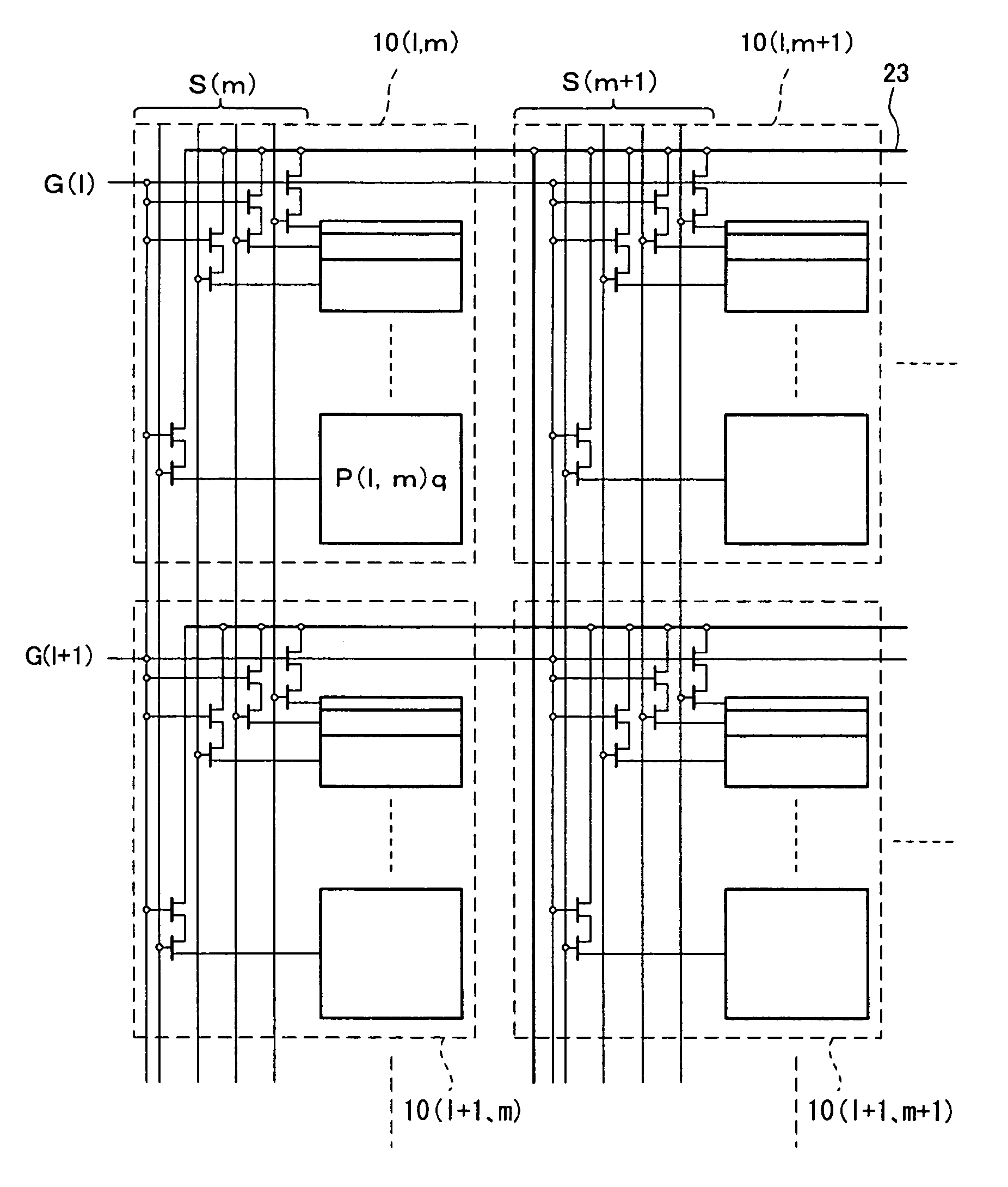
[0024]The following will describe a liquid crystal display of the present embodiment with reference to FIGS. 1 and 2.

[0025]The liquid crystal display of the present embodiment is an active matrix liquid crystal display adopting TFT (Thin Film Transistor) elements.

[0026]In the active matrix liquid crystal display, as FIG. 1 shows, liquid crystal is changed between a pair of transparent substrates (not illustrated), and pixels 10 are disposed in a matrix manner. Further, the liquid crystal display of the present embodiment reproduces images by means of an area ratio gray scale.

[0027]On one of the pair of substrates, as illustrated in FIG. 1, scanning signal lines G(l) (l=0, 1, 2, . . . ) to which scanning signals are serially supplied from a scanning signal line drive circuit (not illustrated) and data signal lines S(m) (m=0, 1, 2, . . . ) to which data signals are serially supplied from a data signal line drive circuit (not illustrated) are provided in an orthogonal manner. In the vi...

second embodiment

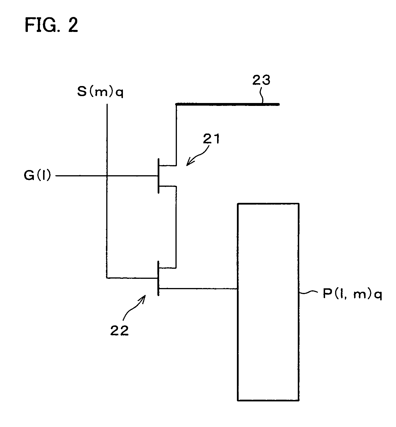
[0041]This embodiment will describe an example of a color liquid crystal display with reference to FIGS. 2–4. By the way, members having the same functions as those described in First Embodiment are given the same numbers, so that the descriptions are omitted for the sake of convenience.

[0042]As FIG. 3 indicates, a liquid crystal display of the present embodiment is identical with the liquid crystal display of First Embodiment, except that the display of the present embodiment includes picture elements 24 each made up of three pixels corresponding to red (R), green (G), and blue (B). Note that, the sub-pixels in each pixel are identical with those of First Embodiment shown in FIG. 2. In the present embodiment, furthermore, data signal lines connected to the respective pixels (R), (G), and (B) of one picture element 24 constitute a single data signal line S(0) (or S(1) . . . ). Also, the pixels of the liquid crystal display, which are connected to one scanning signal line, are also c...

third embodiment

[0048]Next, another example of the color liquid crystal display will be discussed with reference to FIGS. 5 and 6. By the way, members having the same functions as those described in First and Second Embodiments are given the same numbers, so that the descriptions are omitted for the sake of convenience.

[0049]The liquid crystal display of the present embodiment is, as in FIG. 5, includes picture elements 24 each made up of three pixels corresponding to red (R), green (G), and blue (B), as in the case of the liquid crystal display 2 in Second Embodiment. In this manner, to reproduce color images, a black mask and R, G, and B color filters are provided on a substrate on which sub-pixel electrodes are not provided, and the black mask and R, G, and B color filters correspond to respective pixels. In the present liquid crystal display, furthermore, pixels connected to one scanning signal line are alternately connected to a TFT common line 23a and a TFT common line 23b in the direction pa...


PUM


Abstract

The present invention aims at providing a liquid crystal display which can reproduce images in a uniform manner. In a liquid crystal display which adopts an area ratio gray scale and includes pixels each having a plurality of sub-pixels, the sub-pixel includes a sub-pixel electrode and two TFTs, and is connected to a common line to which a predetermined voltage is applied. To the source electrode and drain electrode of one TFT, the drain electrode of the other TFT and the sub-pixel electrode are connected, respectively. To the source electrode of the other TFT, either a scanning signal line or a data signal line is connected. Meanwhile, to the gate electrode of said one TFT, either the scanning signal line or the data signal line which is not connected to the gate electrode of the other TFT is connected.

Description

[0001]This Nonprovisional application claims priority under 35 U.S.C. § 119(a) on Patent Application No. 2002 / 375665 filed in Japan on Dec. 25, 2002, the entire contents of which are hereby incorporated by reference.FIELD OF THE INVENTION[0002]The present invention relates to a liquid crystal display, and more particularly to a liquid crystal display adopting a digital-drive area ratio gray scale.BACKGROUND OF THE INVENTION[0003]In conventional TFT liquid crystal panels, the reversal of a liquid crystal element is controlled by applying an analog voltage to a pixel electrode using a D / A converting source driver. As a result of upsizing, such liquid crystal panels have headaches in, for instance, moving image characteristics (speed of response), viewing angle, luminance shifting and angle shifting of colors, V-T accuracy, and uniformity of in-plane luminance distribution. These problems are caused by the following two electrical issues.[0004]The capacitive driving force and the accur...

Claims


Application Information

Patent Timeline
IPC IPC(8): G09G5/02G09G3/36G02F1/1343G02F1/133G02F1/136G02F1/1368G09G3/20H01L29/786H04N5/66
CPCG09G3/3607G09G3/3659G09G3/2074G09G3/3614G09G2330/02G09G2300/0814G09G2320/0223G09G2320/0233G02F1/133
Inventor YO, SEIJI
Owner SHARP KK
Why Eureka
Try Eureka